- 您现在的位置:买卖IC网 > PDF目录67337 > 5962-9466201MJA (NATIONAL SEMICONDUCTOR CORP) SERIAL INPUT LOADING, 1.8 us SETTLING TIME, 10-BIT DAC, CDIP24 PDF资料下载
参数资料
| 型号: | 5962-9466201MJA |
| 厂商: | NATIONAL SEMICONDUCTOR CORP |
| 元件分类: | DAC |
| 英文描述: | SERIAL INPUT LOADING, 1.8 us SETTLING TIME, 10-BIT DAC, CDIP24 |
| 封装: | CERAMIC, DIP-24 |
| 文件页数: | 9/14页 |
| 文件大小: | 472K |
| 代理商: | 5962-9466201MJA |
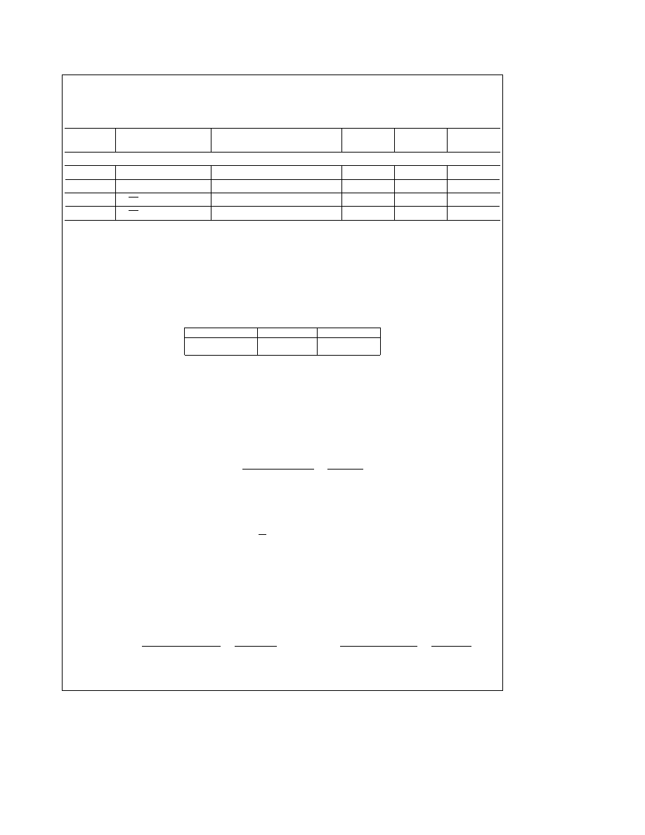
Converter Electrical Characteristics (Continued)
The following specifications apply for AVCC e DVCC e 5V VREF e 265V VBIAS e 14V RL e 2kX (RL is the load resistor on
the analog outputs – pins 2 13 17 and 23) and fCLK e 10 MHz unless otherwise specified Boldface limits apply for TA
e
TJ from TMIN to TMAX All other limits apply for TA e 25 C
Symbol
Parameter
Conditions
Typical
Limit
Units
(Note 3)
(Note 4)
(Limits)
AC ELECTRICAL CHARACTERISTICS
(Continued)
tCZ1
Output Hi-Z to Valid 1
fCLK e 5 MHz
70
ns (max)
tCZ0
Output Hi-Z to Valid 0
fCLK e 5 MHz
70
ns (max)
t1H
CS to Output Hi-Z
10 kX with 60 pF fCLK e 5 MHz
150
ns (max)
t0H
CS to Output Hi-Z
10 kX with 60 pF fCLK e 5 MHz
130
ns (max)
Note 1
Absolute Maximum Ratings indicate limits beyond which damage to the device may occur Operating Ratings indicate conditions for which the device is
functional These ratings do not guarantee specific performance limits however For guaranteed specifications and test conditions see the Converter Electrical
Characteristics The guaranteed specifications apply only for the test conditions listed Some performance characteristics may degrade when the device is not
operated under the listed test conditions
Note 2
All voltages are measured with respect to ground unless otherwise specified
Note 3
When the input voltage (VIN) at any pin exceeds the power supply rails (VIN k GND or VIN l Va) the absolute value of current at that pin should be limited
to 5 mA or less
Note 4
The sum of the currents at all pins that are driven beyond the power supply voltages should not exceed 30 mA
Note 5
The maximum power dissipation must be derated at elevated temperatures and is dictated by TJmax (maximum junction temperature) HJA
(package junction to ambient thermal resistance)
and TA (ambient temperature) The maximum allowable power dissipation at any temperature is
PDmax e (TJmax b TA) HJA or the number given in the Absolute Maximum Ratings whichever is lower The table below details TJmax and HJA for the various
packages and versions of the DAC1054
Part Number
TJmax ( C)
HJA ( CW)
DAC1054CIN
125
42
DAC1054CIWM
125
57
Note 6
Human body model 100 pF discharged through a 15 kX resistor
Note 7
See AN450 ‘‘Surface Mounting Methods and Their Effect on Production Reliability’’ of the section titled ‘‘Surface Mount’’ found in any current Linear
Databook for other methods of soldering surface mount devices
Note 8
Typicals are at TJ e 25 C and represent most likely parametric norm
Note 9
Limits are guaranteed to National’s AOQL (Average Outgoing Quality Level)
Note 10
A monotonicity of 10 bits for the DAC1054 means that the output voltage changes in the same direction (or remains constant) for each increase in the
input code
Note 11
Integral linearity error is the maximum deviation of the output from the line drawn between zero and full-scale (excluding the effects of zero error and full-
scale error)
Note 12
Full-scale error is measured as the deviation from the ideal 2800V full-scale output when VREF e 2650V and VBIAS e 1400V
Note 13
Full-scale error tempco and zero error tempco are defined by the following equation
Error tempco e
Error (TMAX) b Error (TMIN)
VSPAN
(
106
TMAX b TMIN
(
where Error (TMAX) is the zero error or full-scale error at TMAX (in volts) and Error (TMIN) is the zero error or full-scale error at TMIN (in volts) VSPAN is the output
voltage span of the DAC1054 which depends on VBIAS and VREF
Note 14
Zero error is measured as the deviation from the ideal 0302V output when VREF e 2650V VBIAS e 1400V and the digital input word is all zeros
Note 15
Power Supply Sensitivity is the maximum change in the offset error or the full-scale error when the power supply differs from its optimum 5V by up to
050V (10%) The load resistor RL e 2kX
Note 16
Positive or negative settling time is defined as the time taken for the output of the DAC to settle to its final full-scale or zero output to within g05 LSB
This time shall be referenced to the 50% point of the positive edge of CS which initiates the update of the analog outputs
Note 17
Digital crosstalk is the glitch measured on the output of one DAC while applying an all 0s to all 1s transition at the input of the other DACs
Note 18
All DACs have full-scale outputs latched and DI is clocked with no update of the DAC outputs The glitch is then measured on the DAC outputs
Note 19
Clock feedthrough is measured for each DAC with its output at full-scale The serial clock is then applied to the DAC at a frequency of 10 MHz and the
glitch on each DAC full-scale output is measured
Note 20
Channel-to-channel isolation is a measure of the effect of a change in one DAC’s output on the output of another DAC The VREF of the first DAC is varied
between 14V and 265V at a frequency of 15 kHz while the change in full-scale output of the second DAC is measured The first DAC is loaded with all 0s
Note 21
Glitch energy is the difference between the positive and negative glitch areas at the output of the DAC when a 1 LSB digital input code change is applied
to the input The glitch energy will have its largest value at one of the three major transitions The peak value of the maximum glitch is separately specified
Note 22
Power Supply Rejection Ratio is measured by varying AVCC e DVCC between 450V and 550V with a frequency of 10 kHz and measuring the proportion
of this signal imposed on a full-scale output of the DAC under consideration
Note 23
The bandgap reference tempco is defined by the largest value from the following equations
Tempco (TMAX) e
VREF (TMAX) b VREF (TROOM)
VREF (TROOM)
(
106
TMAX b TROOM
( orTempco(TMIN)e VREF(TMIN)bVREF(TROOM)
VREF (TROOM)
(
106
TROOM b TMIN
(
where TROOM e 25 C VREF (TMAX) is the reference output at TMAX and similarly for VREF (TMIN) and VREF (TROOM)
Note 24
A Military RETS specification is available upon request
4
Obsolete
相关PDF资料 |
PDF描述 |
|---|---|
| 5962-9466401MEA | PHASE LOCKED LOOP, 1.4 MHz, CDIP16 |
| 5962-9466401MEX | PHASE LOCKED LOOP, CDIP16 |
| 5962-9466401MEA | PHASE LOCKED LOOP, CDIP16 |
| 5962-9064001CA | QUAD 1-CHANNEL, SGL POLE SGL THROW SWITCH, CDIP14 |
| 7901502EA | 4-CHANNEL, DIFFERENTIAL MULTIPLEXER, CDIP16 |
相关代理商/技术参数 |
参数描述 |
|---|---|
| 59629466401MEA | 制造商:TI 功能描述:CD4046BF3A |
| 5962-9466401MEA | 制造商:Texas Instruments 功能描述:PLL Single 0.3MHz to 2.4MHz 16-Pin CDIP Tube 制造商:Texas Instruments 功能描述:CD4046BF3A - Rail/Tube |
| 5962-9466902Q9C | 制造商:Texas Instruments 功能描述:DSP FLOATING PT 32BIT 40MHZ 25MIPS XCEPT - Gel-pak, waffle pack, wafer, diced wafer on film |
| 5962-9466902QXA | 制造商:Rochester Electronics LLC 功能描述:- Bulk 制造商:Texas Instruments 功能描述:DSP FLOATING PT 32BIT 40MHZ 20MIPS 325CPGA - Rail/Tube |
| 5962-9466902QXC | 制造商:Rochester Electronics LLC 功能描述:- Bulk |
发布紧急采购,3分钟左右您将得到回复。