- 您现在的位置:买卖IC网 > PDF目录56743 > 5962-9470301MXA (ANALOG DEVICES INC) 2-CH 8-BIT PROPRIETARY METHOD ADC, PARALLEL ACCESS, CDIP48 PDF资料下载
参数资料
| 型号: | 5962-9470301MXA |
| 厂商: | ANALOG DEVICES INC |
| 元件分类: | ADC |
| 英文描述: | 2-CH 8-BIT PROPRIETARY METHOD ADC, PARALLEL ACCESS, CDIP48 |
| 封装: | CERAMIC, DIP-48 |
| 文件页数: | 6/9页 |
| 文件大小: | 154K |
| 代理商: | 5962-9470301MXA |
REV. B
AD9058
–6–
18
RZ1
28
ANALOG
IN B
±0.125 V
AD9618
400
50
5k
ANALOG
IN A
±0.125 V
AD580
1
3
2
10k
0.1F
1/2
AD708
+5V
20k
+VREF A
ENCODE
A
ENCODE
B
AD9618
400
50
1/2
AD708
5
20k
3
43
8
38
10
150
10
10pF
1k
50k
5, 9, 22,
24, 37, 41
+5V
RZ2
D0A (LSB)
D7A (MSB)
D0B (LSB)
D7B (MSB)
8
74ACT
273
8
74ACT
273
CLOCK
–VS
7, 20,
26, 39
0.1F
1N4001
4,19, 21
25, 27, 42
RZ1, RZ2 = 2,000
SIP (8/PKG)
ENCODE
10
36
2N3904
0.1F
+1V
±1V
–1V
2N3906
±1 V
0.1F
COMP
1
0.1F
6
40
AD9058
(J-LEAD)
74ACT04
5V
–
+
–
+
–
+
–
+
17
16
15
14
13
12
11
29
30
31
32
33
34
35
5V
–
(SEE TEXT)
+VREF B
AIN A
–VREF A
–VREF B
AIN B
+VS
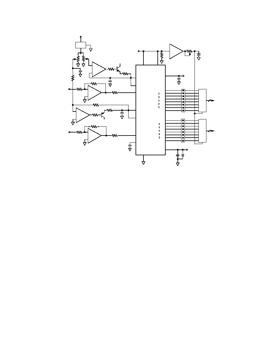
Figure 3. AD9058 Using External Voltage References
The AD9058 offers considerable flexibility in selecting the ana-
log input ranges of the ADCs; the two independent ADCs can
even have different input ranges if required. In Figure 3 above,
the AD9058 is shown configured for
±1 V operation.
The Reference Ladder Offset shown in the specifications table re-
fers to the error between the voltage applied to the +VREF (top)
or –VREF (bottom) of the reference ladder and the voltage re-
quired at the analog input to achieve a 1111 1111 or 0000 0000
transition. This indicates the amount of adjustment range which
must be designed into the reference circuit for the AD9058.
The diode shown between ground and –VS is normally reverse
biased and is used to prevent latch-up. Its use is recommended
for applications in which power supply sequencing might allow
+VS to be applied before –VS; or the +VS supply is not current
limited. If the negative supply is allowed to float (the +5 V sup-
ply is powered up before the –5 V supply), substantial +5 V
supply current will attempt to flow through the substrate (VS
supply contact) to ground. If this current is not limited to <500
mA, the part may be destroyed. The diode prevents this poten-
tially destructive condition from occurring.
Timing
Refer to the AD9058 Timing Diagram. The AD9058 provides
latched data outputs with no pipeline delay. To conserve power,
the data outputs have relatively slow rise and fall times. When
designing system timing, it is important to observe (1) set-up
and hold times; and (2) the intervals when data is changing.
Figure 3 shows 2 k
pull-down resistors on each of the D0–D7
output data bits. When operating at conversion rates higher than
40 MSPS, these resistors help equalize rise and fall times and
ease latching the output data into external latches. The 74ACT
logic family devices have short set-up and hold times and are the
recommended choices for speeds of 40 MSPS or more.
Layout
To insure optimum performance, a single low-impedance ground
plane is recommended. Analog and digital grounds should be
connected together and to the ground plane at the AD9058 de-
vice. Analog and digital power supplies should be bypassed to
ground through 0.1
F ceramic capacitors as close to the unit as
possible.
An evaluation board (ADI part #AD9058/PCB) is available to
aid designers and provide a suggested layout. The use of sockets
may limit the dynamic performance of the part and is not rec-
ommended except for prototype or evaluation purposes.
For prototyping or evaluation, surface mount sockets are available
from Methode (part #213-0320602) for evaluating AD9058 sur-
face mount packages. To evaluate the AD9058 in through-hole
PCB designs, use the AD9058JD/KD with individual pin sockets
(AMP part #6-330808-0). Alternatively, surface mount AD9058
units can be mounted in a through-hole socket (Circuit Assembly
Corporation, Irvine California part #CA-44SPC-T).
AD9058 APPLICATIONS
Combining two ADCs in a single package is an attractive alter-
native in a variety of systems when cost, reliability and space are
important considerations. Different systems emphasize particu-
lar specifications, depending on how the part is used.
In high density digital radio communications, a pair of high
speed ADCs are used to digitize the in-phase (I) and quadrature
(Q) components of a modulated signal. The signal presented to
each ADC in this type of system consists of message-dependent
amplitudes varying at the symbol rate, which is equal to the
sample rates of the converters.
相关PDF资料 |
PDF描述 |
|---|---|
| 5962-9470301MYX | DUAL 1-CH 8-BIT PROPRIETARY METHOD ADC, PARALLEL ACCESS, CQCC44 |
| 5962-9470301MXX | DUAL 1-CH 8-BIT PROPRIETARY METHOD ADC, PARALLEL ACCESS, CDIP48 |
| 5962-9474301MXA | 1-CH 16-BIT SUCCESSIVE APPROXIMATION ADC, PARALLEL ACCESS, CDIP28 |
| 5962-9474301MXX | 1-CH 16-BIT SUCCESSIVE APPROXIMATION ADC, PARALLEL ACCESS, CDIP28 |
| 5962-9474601QEA | STEPPER MOTOR CONTROLLER, 1 A, CDIP16 |
相关代理商/技术参数 |
参数描述 |
|---|---|
| 5962-9470301MYA | 制造商:Analog Devices 功能描述:ADC DUAL FLASH 50MSPS 8BIT PARALLEL 44PIN JLCC - Rail/Tube |
| 5962-9470401QXA | 制造商:Texas Instruments 功能描述:FIFO Mem Sync Dual Bi-Dir 512 x 18 x 2 84-Pin CPGA |
| 5962-9471601H4A | 制造商:Micross Components, Inc. 功能描述:FLASH-MCM,4 MB - Trays |
| 5962-9471601H8C | 制造商:Microsemi Corporation 功能描述:128K X 32 FLASH MODULE, 5V, 150NS, NO CONNECT, 66 PGA 1.075" - Bulk 制造商:White Electronic Designs 功能描述:128K X 32 FLASH MODULE, 5V, 150NS, NO CONNECT, 66 PGA 1.075" - Bulk |
| 5962-9471601HAA | 制造商:Micross Components 功能描述:FLASH-MCM,4 MB - Trays |
发布紧急采购,3分钟左右您将得到回复。