- 您现在的位置:买卖IC网 > PDF目录91416 > 5962-9751801MPA (NATIONAL SEMICONDUCTOR CORP) OP-AMP, CDIP8 PDF资料下载
参数资料
| 型号: | 5962-9751801MPA |
| 厂商: | NATIONAL SEMICONDUCTOR CORP |
| 元件分类: | 运算放大器 |
| 英文描述: | OP-AMP, CDIP8 |
| 封装: | DIP-8 |
| 文件页数: | 4/8页 |
| 文件大小: | 316K |
| 代理商: | 5962-9751801MPA |
General Design Equations
The CLC440 is a unity gain stable voltage feedback
amplifier. The matched input bias currents track well over
temperature. This allows the DC offset to be minimized
by matching the impedance seen by both inputs.
Gain
The non-inverting and inverting gain equations for the
CLC440 are as follows:
Non-inverting Gain:
Inverting Gain:
Gain Bandwidth Product
The CLC440 is a voltage feedback amplifier, whose
closed-loop bandwidth is approximately equal to the
gain-bandwidth product (GBP) divided by the gain (Av).
For gains greater than 5, Av sets the closed-loop band-
width of the CLC440.
Closed Loop Bandwidth =
GBP = 230MHz
For gains less than 5, refer to the frequency response
plots to determine maximum bandwidth.
Output Drive and Settling Time Performance
The CLC440 has large output current capability. The
90mA of output current makes the CLC440 an excellent
choice for applications such as:
Video Line Drivers
Distribution Amplifiers
When driving a capacitive load or coaxial cable, include a
series resistance Rs to back match or improve settling
time. Refer to the “Settling Time vs. Capacitive Load” plot
in the typical performance section to determine the
recommended resistance for various capacitive loads.
When driving resistive loads of under 500
, settling time
performance diminishes. This degradation occurs
because a small change in voltage on the output causes
a large change of current in the power supplies. This
current creates ringing on the power supplies. A small
resistor will dampen this effect if placed in series with the
6.8
F bypass capacitor.
Noise Figure
Noise Figure (NF) is a measure of noise degradation
caused by an amplifier.
where,
eni = Total Equivalent Input Noise Density
Due to the Amplifier
et = Thermal Voltage Noise (
seq)
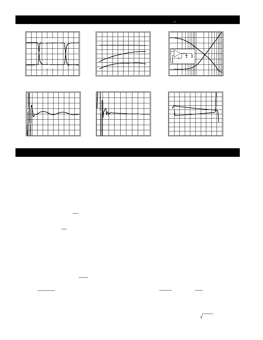
CLC440 Typical Performance Characteristics (A
V = +2, Rf = 250:Vcc = + 5V, RL = 100 unless specified)
Ib and Ios vs. Common-Mode Voltage
Offset
Current,
I
os
(5nA/div
)
Bias
Current,
I
b (0.5
A/div)
Common-Mode Input Voltage (V)
-4.0
-2.4
2.4
0
4.0
0
-0.8
0.8
Ib
los
-10
-20
10
20
2.0
1.0
-1.0
-2.0
APPLICATION INFORMATION
Pulse Response
Output
Voltage
(0.5V/div)
Time (5ns/div)
2.0
1.0
-1.0
-2.0
0
AV = +2
AV = -2
0.05% Settling Time vs. Capacitive Load
Settling
Time,
T
s(ns)
to
0.05%
10
100
1000
Load Capacitance CL (pF)
80
60
40
20
0
Recommended
R
s (
)
55
45
35
25
15
+
-
Rs
1k
CL
Rs
Ts
Short Term Settling Time
Settling
Error
%
of
Output
Step
Time (ns)
0
20
80
0.1
100
40
60
0.2
0
-0.1
-0.2
Long Term Settling Time
Settling
Error
%
of
Output
Step
Time (s)
10
-9
10
-7
10
-1
0.1
10
0
10
-5
10
-3
0.2
0
-0.1
-0.2
10
-2
10
-4
10
-6
10
-8
1
R
f
g
+
R
f
g
GBP
Av
A
RR
R
v
f
g
=
+
()
NF
10LOG
S/N
10LOG
e
ii
oo
ni
2
t
2
=
=
4kTR
Typical DC Errors vs. Temperature
Input
Offset
Voltage,
V
io
(mV)
Input
Bias,
Offset
Current,
l
b l
os
(
A)
Temperature (C
°)
0.4
0
-60
-20
100
-0.8
-1.6
-0.4
140
6
2
-6
-14
-2
-1.2
20
60
-10
los
lb
Vio
http://www.national.com
4
相关PDF资料 |
PDF描述 |
|---|---|
| 5962-9763301QGA | DUAL OP-AMP, 5000 uV OFFSET-MAX, 0.6 MHz BAND WIDTH, MBCY8 |
| 5962-9763301QGX | DUAL OP-AMP, 5000 uV OFFSET-MAX, 0.6 MHz BAND WIDTH, MBCY8 |
| 5962D9567002VCX | OP-AMP, 1 MHz BAND WIDTH, CDIP14 |
| 5962D9568802VPX | OP-AMP, 7000 uV OFFSET-MAX, CDIP8 |
| 5962F0254201V9A | QUAD OP-AMP, 10000 uV OFFSET-MAX, UUC12 |
相关代理商/技术参数 |
参数描述 |
|---|---|
| 5962-9752001MPA | 制造商:Texas Instruments 功能描述:OP Amp Single Current Fdbk 8-Pin CDIP |
| 5962-9752401QXC | 制造商:Xilinx 功能描述: |
| 5962-9752601Q2A | 制造商:Texas Instruments 功能描述:Decoder/Demultiplexer Single 3-to-8 20-Pin LCCC Tube |
| 5962-9752601QFA | 制造商:Texas Instruments 功能描述:Decoder/Demultiplexer Single 3-to-8 16-Pin CFPAK Tube |
| 5962-9752701Q3A | 制造商:Texas Instruments 功能描述:Bus Switch 2-Element CMOS 10-IN 28-Pin LCCC Tube 制造商:Texas Instruments 功能描述:BUS SWIT 2-ELEM 5-IN 28LCCC - Rail/Tube |
发布紧急采购,3分钟左右您将得到回复。