- 您现在的位置:买卖IC网 > PDF目录293971 > 5962H9215315QMA 32K X 8 STANDARD SRAM, 70 ns, CDIP28 PDF资料下载
参数资料
| 型号: | 5962H9215315QMA |
| 元件分类: | SRAM |
| 英文描述: | 32K X 8 STANDARD SRAM, 70 ns, CDIP28 |
| 封装: | 0.600 X 1.400 INCH, 2.54 MM PITCH, SIDE BRAZED, CERAMIC, DIP-28 |
| 文件页数: | 8/15页 |
| 文件大小: | 144K |
| 代理商: | 5962H9215315QMA |
2
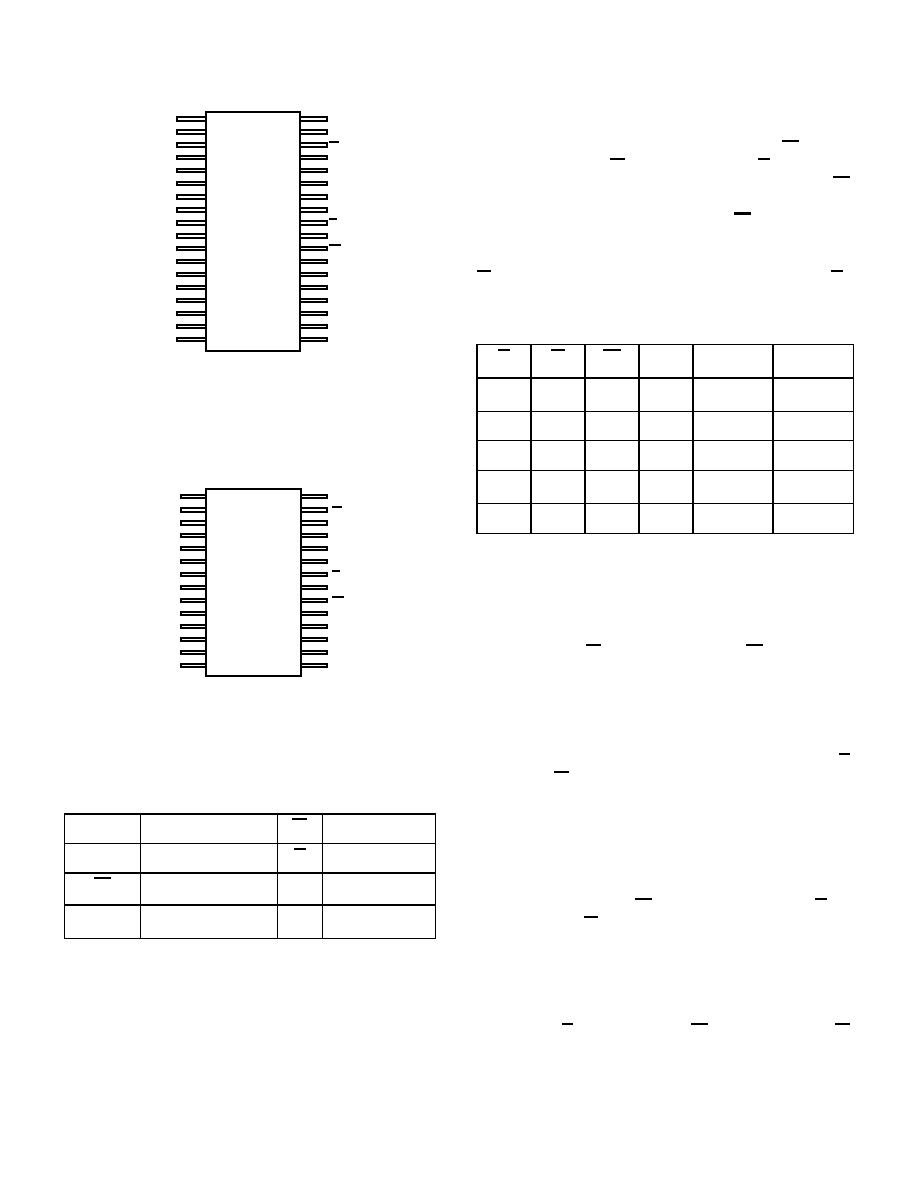
PIN NAMES
1. 36-lead flatpack only.
DEVICE OPERATION
The UT7156 has four control inputs called Enable 1 (E1), Enable
2 (E2), Write Enable (W), and Output Enable (G); 15 address
inputs, A(14:0); and eight bidirectional data lines, DQ(7:0). E1
and E2 are device enable inputs that control device selection,
active, and standby modes. Asserting both E1 and E2 enables
the device, causes I
DD to rise to its active value, and decodes the
15 address inputs to select one of 32,768 words in the memory.
W controls read and write operations. During a read cycle, G
must be asserted to enable the outputs.
Table 1. Device Operation Truth Table
Notes:
1. “X” is defined as a “don’t care” condition.
2. Device active; outputs disabled.
3. Tied active (i.e., logic 1) in the 28-pin DIP package.
READ CYCLE
A combination of W greater than VIH (min), E1 less than VIL
(max), and E2 greater than VIH (min) defines a read cycle. Read
access time is measured from the latter of device enable, output
enable, or valid address to valid data output.
Read Cycle 1, the Address Access read in figure 3a, is initiated
by a change in address inputs while the chip is enabled with G
asserted and W deasserted. Valid data appears on data outputs
DQ(7:0) after the specified tAVQV is satisfied. Outputs remain
active throughout the entire cycle. As long as device enable and
output enable are active, the address inputs may change at a rate
equal to the minimum read cycle time (tAVAV).
Read Cycle 2, the Chip Enable-controlled Access in figure 3b,
is initiated by the latter of E1 and E2 going active while G
remains asserted, W remains deasserted, and the addresses
remain stable for the entire cycle. After the specified tETQV is
satisfied, the eight-bit word addressed by A(14:0) is accessed
and appears at the data outputs DQ(7:0).
Read Cycle 3, the Output Enable-controlled Access in figure 3c,
is initiated by G going active while E1 and E2 are asserted, W
is deasserted, and the addresses are stable. Read access time is
tGLQV unless tAVQV or tETQV have not been satisfied.
A(14:0)
Address
W
Write
DQ(7:0)
Data Input/Output
G
Output Enable
E1
Enable 1
VDD Power
E21
Enable 2
VSS
Ground
1
36
2
35
3
34
4
33
5
32
6
31
7
30
8
29
9
28
10
27
11
26
12
25
13
24
14
23
15
22
16
21
17
20
18
19
Figure 2a. SRAM Pinout (36)
VSS
VDD
W
E2
A13
A8
A9
A11
G
A10
E1
DQ7
DQ6
DQ5
DQ4
DQ3
VDD
VSS
VDD
A14
A12
A7
A6
A5
A4
A3
A2
A1
A0
DQ0
DQ1
DQ2
NC
VDD
VSS
Figure 2b. SRAM Pinout (28)
1
28
2
27
3
26
4
25
5
24
6
23
7
22
8
21
9
20
10
19
11
18
12
17
13
16
14
15
VDD
W
A13
A8
A9
A11
G
A10
E1
DQ7
DQ6
DQ5
DQ4
DQ3
A14
A12
A7
A6
A5
A4
A3
A2
A1
A0
DQ0
DQ1
DQ2
VSS
G
W
E1
E23
I/O Mode
Mode
X1
X
0
3-state
Standby
X
1
X
3-state
Standby
X
0
1
Data in
Write
1
0
1
3-state
Read
2
0
1
0
1
Data out
Read
相关PDF资料 |
PDF描述 |
|---|---|
| 5962R9581901QQX | 24 I/O, PIA-GENERAL PURPOSE, CDIP40 |
| 59K16A-102T4 | CABLE TERMINATED, FEMALE, RF CONNECTOR, CRIMP, JACK |
| 59K16A-106T4 | CABLE TERMINATED, FEMALE, RF CONNECTOR, CRIMP, JACK |
| 59K16A-109T4 | CABLE TERMINATED, FEMALE, RF CONNECTOR, CRIMP, JACK |
| 59K16A-1M4T4 | CABLE TERMINATED, FEMALE, RF CONNECTOR, CRIMP, JACK |
相关代理商/技术参数 |
参数描述 |
|---|---|
| 5962H94A0305QXC | 制造商: 功能描述: 制造商:undefined 功能描述: |
| 5962H9853701 | 制造商: 功能描述: 制造商:undefined 功能描述: |
| 5962L0051502VHA | 制造商:Analog Devices 功能描述:AEROSPACE 7NS SINGLE COMPARATOR - Trays |
| 5962L0052401VGA | 功能描述:校验器 IC RoHS:否 制造商:STMicroelectronics 产品: 比较器类型: 通道数量: 输出类型:Push-Pull 电源电压-最大:5.5 V 电源电压-最小:1.1 V 补偿电压(最大值):6 mV 电源电流(最大值):1350 nA 响应时间: 最大工作温度:+ 125 C 安装风格:SMD/SMT 封装 / 箱体:SC-70-5 封装:Reel |
| 5962L0052401VHA | 功能描述:校验器 IC RoHS:否 制造商:STMicroelectronics 产品: 比较器类型: 通道数量: 输出类型:Push-Pull 电源电压-最大:5.5 V 电源电压-最小:1.1 V 补偿电压(最大值):6 mV 电源电流(最大值):1350 nA 响应时间: 最大工作温度:+ 125 C 安装风格:SMD/SMT 封装 / 箱体:SC-70-5 封装:Reel |
发布紧急采购,3分钟左右您将得到回复。