- 您现在的位置:买卖IC网 > PDF目录293971 > 5962R0150202VYX 16-BIT, 16 MHz, RISC PROCESSOR, QFP132 PDF资料下载
参数资料
| 型号: | 5962R0150202VYX |
| 元件分类: | 微控制器/微处理器 |
| 英文描述: | 16-BIT, 16 MHz, RISC PROCESSOR, QFP132 |
| 封装: | FP-132 |
| 文件页数: | 13/53页 |
| 文件大小: | 458K |
| 代理商: | 5962R0150202VYX |
第1页第2页第3页第4页第5页第6页第7页第8页第9页第10页第11页第12页当前第13页第14页第15页第16页第17页第18页第19页第20页第21页第22页第23页第24页第25页第26页第27页第28页第29页第30页第31页第32页第33页第34页第35页第36页第37页第38页第39页第40页第41页第42页第43页第44页第45页第46页第47页第48页第49页第50页第51页第52页第53页
20
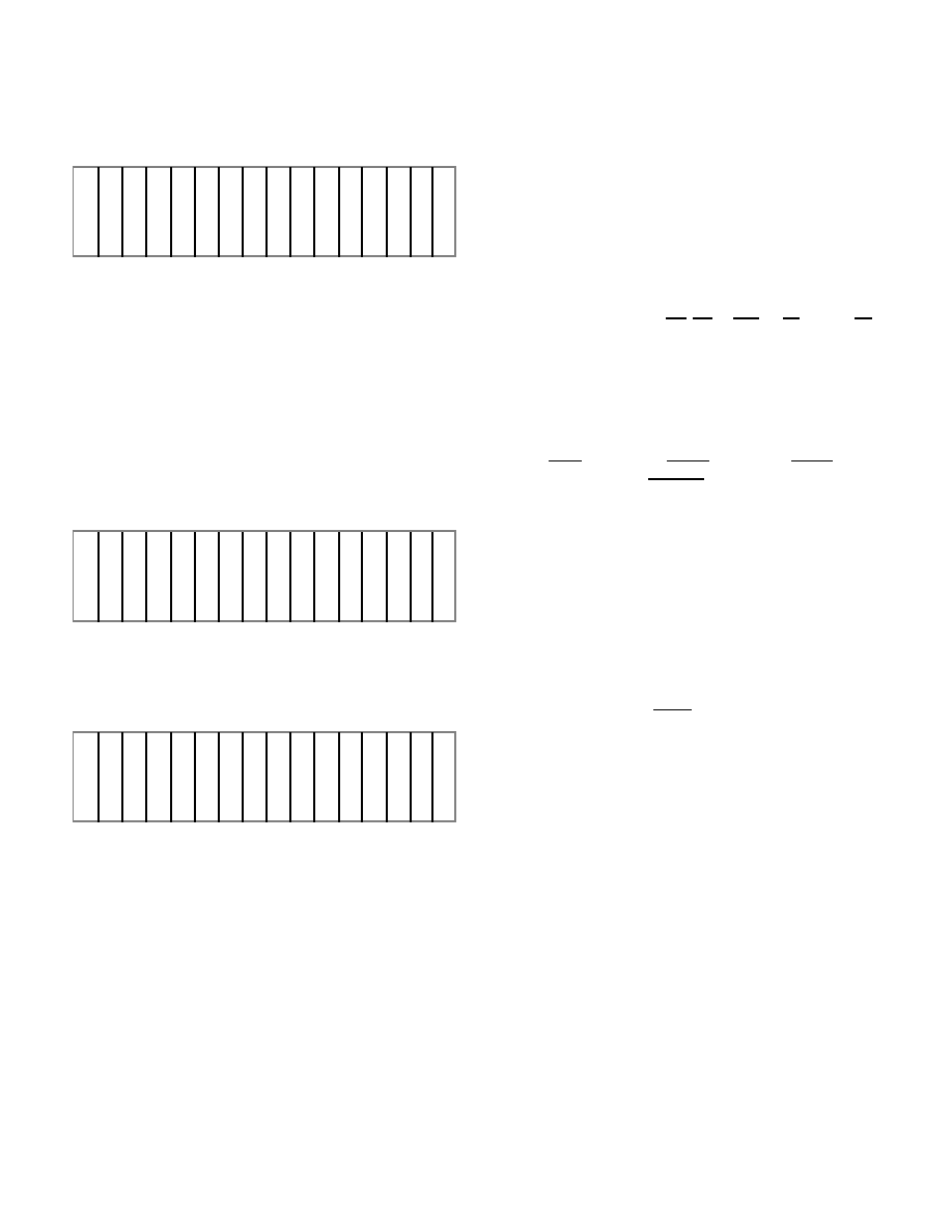
Program Counter Register (PC)
The Program Counter Register (PC) (figure 23) contains the 16-
bit address for the present MIL-STD-1750A instruction. The
RISC I/O instruction reads from or writes to the PC.
1750 Timer A (TA) and 1750 Timer B (TB)
The Timer A (TA) and Timer B (TB) registers, figures 24a and
24b respectively, are 16-bit binary counters as defined by MIL-
STD-1750A. The RISC I/O instruction starts, halts, reads, and
loads them. When one of the timers reaches its programmed
time setting, such as going from FFFFH to 0000H, a timeout
occurs. This timeout sets the appropriate bit in the Pending
Interrupt Register (PI).
SYSTEM INTERFACE
The System Interface describes how the Instruction and
Operand address and data busses operate during the
UT1750AR’s many machine cycles and bus operations. The
discussion about the UT1750AR’s machine cycles and bus
operations applies to both the RISC mode and the MIL-STD-
1750A mode of operation, since in the 1750 mode of operation
the UT1750AR executes a specialized set of RISC macros that
allow the UT1750AR to emulate the MIL-STD-1750A
Instruction Set Architecture.
The UT1750AR has the following seven types of machine
operations or bus cycle operations:
Data Bus Cycle Operation
DMA Operation and Bus Arbitration
Interrupt Operation and Exception Handling
RISC Instruction Bus Cycle Operation
Internal UART Operation
Console Mode of Operation
1750 Instruction Memory Mapping
Operand Bus and Instruction Bus Interfaces
The UT1750AR Operand Data Bus interface supports multiple
processor and Direct Memory Access (DMA) configurations.
The Operand Address Bus (A15-A0), Data Bus (D15-D0), and
memory control bus signals ( AS, DS, R/WR, M/IO, and OP/IN)
are TTL-compatible signals that may be placed in a high-
impedance state. These signals are only active during bus cycles
when the UT1750AR is the current bus master. On other bus
cycles, these signals enter a high-impedance state so an alternate
bus master can control the busses.
The four signals that make up the Arbitration Control Bus -- Bus
Request (BRQ), Bus Grant (BGNT), Bus Busy (BUSY), and
Bus Grant Acknowledge ( BGACK) -- control the UT1750AR’s
Operand Data Bus arbitration process. The arbitration process
allows asynchronous bus arbitration.
The Instruction Bus does not allow any type of bus arbitration.
The UT1750AR is the only device permitted to access
Instruction memory; this access is generally confined to reading
RISC instructions the UT1750AR subsequently executes,
although the RISC instruction set does provide one instruction
the UT1750AR uses to alter RISC memory. This instruction is
the Store Register to Instruction Memory (STRI).
The Instruction address and data busses only enter a high-
impedance state when the TEST input is low.
A TYPICAL UT1750AR BUS CYCLE
Figure 25a (see page 21), a generalized diagram for a typical
UT1750AR bus cycle, shows the UT1750AR’s bus cycle
separated into four distinct time periods (CK1 through CK4).
These time periods are based on the processor clock. The
UT1750AR performs a separate function during each of these
four time periods.
15 14 13 12 11 10 9
8
7
5
4
3 2
1 0
P
C
1
5
P
C
1
4
P
C
1
3
P
C
1
2
P
C
1
P
C
1
0
P
C
9
P
C
8
6
P
C
6
P
C
7
P
C
5
P
C
4
P
C
3
P
C
2
P
C
1
P
C
0
MSB
LSB
Figure 23. The Program Counter Register (PC)
15 14 13 12 11 10 9
8
7
5
4
3 2
1 0
T
A
1
5
T
A
1
4
T
A
1
3
T
A
1
2
T
A
1
T
A
1
0
T
A
9
T
A
8
6
T
A
6
T
A
7
T
A
5
T
A
4
T
A
3
T
A
2
T
A
1
T
A
0
MSB
LSB
Figure 24a. 1750 Timer A (TA)
15 14 13 12 11 10 9
8
7
5
4
3 2
1 0
T
B
1
5
T
B
1
4
T
B
1
3
T
B
1
2
T
B
1
T
B
1
0
T
B
9
T
B
8
6
T
B
6
T
B
7
T
B
5
T
B
4
T
B
3
T
B
2
T
B
1
T
B
0
MSB
LSB
Figure 24b. 1750 Timer B (TB)
相关PDF资料 |
PDF描述 |
|---|---|
| 5962R0722402VYC | SPECIALTY MICROPROCESSOR CIRCUIT, PQFP256 |
| 5962R8958702VXA | 5 V FIXED POSITIVE LDO REGULATOR, 1 V DROPOUT, CDSO16 |
| 5962R9215311VTA | 32K X 8 STANDARD SRAM, 55 ns, CDFP36 |
| 5962R9215311VTX | 32K X 8 STANDARD SRAM, 55 ns, CDFP36 |
| 5962G9215309VMX | 32K X 8 STANDARD SRAM, 55 ns, CDIP28 |
相关代理商/技术参数 |
参数描述 |
|---|---|
| 5962R0253801VZA | 制造商:Analog Devices 功能描述:- Rail/Tube |
| 5962R0720802VXC | 制造商:Texas Instruments 功能描述:ADS5463 RHA QMLV DEVICE |
| 5962R0722601VZA | 制造商:Texas Instruments 功能描述:D/A CONVERTER, 12-BIT - Trays |
| 5962R0722701VZA | 功能描述:模数转换器 - ADC 8-Ch 50 kSPS-1 MSPS RoHS:否 制造商:Texas Instruments 通道数量:2 结构:Sigma-Delta 转换速率:125 SPs to 8 KSPs 分辨率:24 bit 输入类型:Differential 信噪比:107 dB 接口类型:SPI 工作电源电压:1.7 V to 3.6 V, 2.7 V to 5.25 V 最大工作温度:+ 85 C 安装风格:SMD/SMT 封装 / 箱体:VQFN-32 |
| 5962R0722902VXA | 功能描述:低压差稳压器 - LDO 3-Terminal Adj Reg RoHS:否 制造商:Texas Instruments 最大输入电压:36 V 输出电压:1.4 V to 20.5 V 回动电压(最大值):307 mV 输出电流:1 A 负载调节:0.3 % 输出端数量: 输出类型:Fixed 最大工作温度:+ 125 C 安装风格:SMD/SMT 封装 / 箱体:VQFN-20 |
发布紧急采购,3分钟左右您将得到回复。