- 您现在的位置:买卖IC网 > PDF目录67347 > 5962R0151901TXA (ANALOG DEVICES INC) DUAL 3-CH 12-BIT PROPRIETARY METHOD ADC, PARALLEL ACCESS, CQFP68 PDF资料下载
参数资料
| 型号: | 5962R0151901TXA |
| 厂商: | ANALOG DEVICES INC |
| 元件分类: | ADC |
| 英文描述: | DUAL 3-CH 12-BIT PROPRIETARY METHOD ADC, PARALLEL ACCESS, CQFP68 |
| 封装: | CERAMIC, LCC-68 |
| 文件页数: | 2/24页 |
| 文件大小: | 2403K |
| 代理商: | 5962R0151901TXA |
AD10265
–10–
REV. A
THEORY OF OPERATION
Refer to the Functional Block Diagram. The AD10265 employs
three monolithic ADI components per channel (AD9631,
AD9632, and AD6640), along with multiple passive resistor
networks and decoupling capacitors to fully integrate a complete
12-bit analog-to-digital converter.
The input signal is first passed through a precision laser-trimmed
resistor divider, allowing the user to externally select operation
with a full-scale signal of
±0.5 V, ±1.0 V, or ±2.0 V by choosing
the proper input terminal for the application.
Since the AD6640 implements a true differential analog input,
the AD9631/AD9632 have been configured to provide a differ-
ential input for the AD6640 ADC through ac-coupling. The ac
signal gain of the AD9631/AD9632 can be trimmed to provide a
constant differential input to the AD6640. This allows the
converter to be used in multiple system applications without
the need for external gain circuit normally requiring trim. The
AD9631/AD9632 were chosen for their superior ac performance
and input drive capabilities, which have limited the ability of
many amplifiers to drive high-performance ADCs. As new
amplifiers are developed, pin-compatible improvements are
planned to incorporate the latest operational amplifier technology.
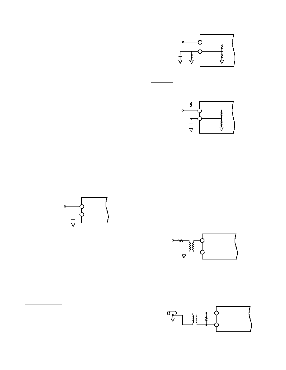
APPLYING THE AD10265
Encoding the AD10265
Best performance is obtained by driving the encode pins differ-
entially. However, the AD10265 is also designed to interface
with TTL and CMOS logic families. The source used to drive
the ENCODE pin(s) must be clean and free from jitter. Sources
with excessive jitter will limit SNR and overall performance.
0.01 F
TTL OR CMOS
SOURCE
ENCODE
AD10265
Figure 6. Single-Ended TTL/CMOS Encode
The AD10265 encode inputs are connected to a differential input
stage (see Figure 4 under Equivalent Circuits). With no input
connected to either ENCODE pin, the voltage divider biases the
inputs to 1.6 V. For TTL or CMOS usage, the encode source
should be connected to ENCODE.
ENCODE should be
decoupled using a low inductance or microwave chip capacitor
to ground.
If a logic threshold other than the nominal 1.6 V is required,
the following equations show how to use an external resistor,
Rx, to raise or lower the trip point (see Figure 4, R1 = 17 k
,
R2 = 8 k
).
V
RR
RRx
R Rx
1
52
12
1
2
=
++
x
to lower logic threshold.
0.01 F
ENCODE
SOURCE
ENCODE
AD10265
Rx
V1
5V
R1
R2
Figure 7. Lower Threshold for Encode
V
R
RRx
1
52
2
1
=
+
to raise logic threshold.
0.01 F
ENCODE
SOURCE
ENCODE
AD10265
Rx
V1
5V
R1
R2
AVCC
Figure 8. Raise Logic Threshold for Encode
While the single-ended encode will work well for many applica-
tions, driving the encode differentially will provide increased
performance. Depending on circuit layout and system noise,
a 1 dB to 3 dB improvement in SNR can be realized. It is
recommended that differential TTL logic be used, however,
because most TTL families that support complementary outputs
are not delay or slew rate matched. Instead, it is recommended
that the encode signal be ac-coupled into the ENCODE and
ENCODE pins.
The simplest option is shown below. The low jitter TTL signal is
coupled with a limiting resistor, typically 100
, to the primary
side of an RF transformer (these transformers are inexpensive
and readily available; part number in Figure 9 is from Mini-
Circuits). The secondary side is connected to the ENCODE
and
ENCODE pins of the converter. Since both encode inputs
are self-biased, no additional components are required.
TTL
ENCODE
AD10265
100
T1–1T
Figure 9. TTL Source—Differential Encode
A clean sine wave may be substituted for a TTL clock. In this
case, the matching network is shown below. Select a transformer
ratio to match source and load impedances. The input impedance
of the AD10265 encode is approximately 11 k
differentially.
Therefore “R,” shown in Figure 10, may be any value that is
convenient for available drive power.
ENCODE
AD10265
R
T1–1T
SINE
SOURCE
Figure 10. Sine Source—Differential Encode
相关PDF资料 |
PDF描述 |
|---|---|
| 5962-9865901HXA | DUAL 3-CH 12-BIT PROPRIETARY METHOD ADC, PARALLEL ACCESS, CQFP68 |
| 5962R0153702QXX | QUAD 2-CHANNEL, CROSS POINT SWITCH, DFP64 |
| 5962G0153702QXC | QUAD 2-CHANNEL, CROSS POINT SWITCH, DFP64 |
| 5962H0153702VXC | QUAD 2-CHANNEL, CROSS POINT SWITCH, DFP64 |
| 5962H0153702VXX | QUAD 2-CHANNEL, CROSS POINT SWITCH, DFP64 |
相关代理商/技术参数 |
参数描述 |
|---|---|
| 5962R0253801VZA | 制造商:Analog Devices 功能描述:- Rail/Tube |
| 5962R0720802VXC | 制造商:Texas Instruments 功能描述:ADS5463 RHA QMLV DEVICE |
| 5962R0722601VZA | 制造商:Texas Instruments 功能描述:D/A CONVERTER, 12-BIT - Trays |
| 5962R0722701VZA | 功能描述:模数转换器 - ADC 8-Ch 50 kSPS-1 MSPS RoHS:否 制造商:Texas Instruments 通道数量:2 结构:Sigma-Delta 转换速率:125 SPs to 8 KSPs 分辨率:24 bit 输入类型:Differential 信噪比:107 dB 接口类型:SPI 工作电源电压:1.7 V to 3.6 V, 2.7 V to 5.25 V 最大工作温度:+ 85 C 安装风格:SMD/SMT 封装 / 箱体:VQFN-32 |
| 5962R0722902VXA | 功能描述:低压差稳压器 - LDO 3-Terminal Adj Reg RoHS:否 制造商:Texas Instruments 最大输入电压:36 V 输出电压:1.4 V to 20.5 V 回动电压(最大值):307 mV 输出电流:1 A 负载调节:0.3 % 输出端数量: 输出类型:Fixed 最大工作温度:+ 125 C 安装风格:SMD/SMT 封装 / 箱体:VQFN-20 |
发布紧急采购,3分钟左右您将得到回复。