- 您现在的位置:买卖IC网 > PDF目录67347 > 5962R0151901TXA (ANALOG DEVICES INC) DUAL 3-CH 12-BIT PROPRIETARY METHOD ADC, PARALLEL ACCESS, CQFP68 PDF资料下载
参数资料
| 型号: | 5962R0151901TXA |
| 厂商: | ANALOG DEVICES INC |
| 元件分类: | ADC |
| 英文描述: | DUAL 3-CH 12-BIT PROPRIETARY METHOD ADC, PARALLEL ACCESS, CQFP68 |
| 封装: | CERAMIC, LCC-68 |
| 文件页数: | 3/24页 |
| 文件大小: | 2403K |
| 代理商: | 5962R0151901TXA |
REV. A
AD10265
–11–
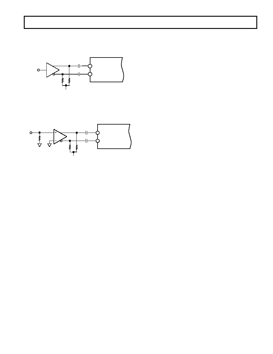
If a low jitter ECL clock is available, another option is to ac-couple
a differential ECL signal to the encode input pins as shown
below. The capacitors shown here should be chip capacitors,
but do not need to be of the low inductance variety.
ENCODE
AD10265
ECL
GATE
0.1 F
–VS
510
Figure 11. Differential ECL for Encode
As a final alternative, the ECL gate may be replaced by an ECL
comparator. The input to the comparator could then be a logic
signal or a sine signal.
ENCODE
AD10265
0.1 F
–VS
50
AD96687 (1/2)
510
Figure 12. ECL Comparator for Encode
USING THE FLEXIBLE INPUT
The AD10265 has been designed with the user’s ease of operation
in mind. Multiple input configurations have been included on
board to allow the user a choice of input signal levels and input
impedance. While the standard inputs are
±0.5 V, ±1.0 V, and
±2.0 V, the user can select the input impedance of the AD10265
on any input by using the other inputs as alternate locations for
GND or an external resistor. The following chart summarizes
the impedance options available at each input location:
AIN1 = 100
when AIN2 and AIN3 Are Open.
AIN1 = 75
when A
IN3 Is Shorted to GND.
AIN1 = 50
when AIN2 Is Shorted to GND.
AIN2 = 200
when AIN3 Is Open.
AIN2 = 100
when A
IN3 Is Shorted to GND.
AIN2 = 75
when AIN2 to AIN3 Has an External Resistor of
AIN2 = 300
, with AIN 3 Shorted to GND.
AIN2 = 50
when A
IN2 to AIN3 Has an External Resistor of
AIN2 = 100
, with AIN3 Shorted to GND.
AIN3 = 400
.
AIN3 = 100
when A
IN3 Has an External Resistor of 133
to GND.
AIN3 = 75
when AIN3 Has an External Resistor of 92 to GND.
AIN3 = 50
when AIN3 Has an External Resistor of 57 to GND.
GROUNDING AND DECOUPLING
Analog and Digital Grounding
Proper grounding is essential in any high speed, high resolution
system. Multilayer printed circuit boards (PCBs) are recom-
mended to provide optimal grounding and power schemes. The
use of ground and power planes offers distinct advantages:
1. The minimization of the loop area encompassed by a signal
and its return path.
2. The minimization of the impedance associated with ground
and power paths.
3. The inherent distributed capacitor formed by the power
plane, PCB insulation, and ground plane.
These characteristics result in both a reduction of electromagnetic
interference (EMI) and an overall improvement in performance.
It is important to design a layout that prevents noise from coupling
to the input signal. Digital signals should not be run in parallel
with input signal traces and should be routed away from the
input circuitry. The AD10265 does not distinguish between
analog and digital ground pins as the AD10265 should always
be treated as an analog component. All ground pins should be
connected together directly under the AD10265. The PCB
should have a ground plane covering all unused portions of the
component side of the board to provide a low impedance path
and manage the power and ground currents. The ground plane
should be removed from the area near the input pins to reduce
stray capacitance.
LAYOUT INFORMATION
The schematic of the evaluation board (Figure 13) represents
a typical implementation of the AD10265. The pinout of the
AD10265 is very straightforward and facilitates ease of use and
the implementation of high frequency/high resolution design
practices. It is recommended that high quality ceramic chip
capacitors be used to decouple each supply pin to ground directly
at the device. All capacitors can be standard high quality ceramic
chip capacitors.
Care should be taken when placing the digital output runs.
Because the digital outputs have such a high slew rate, the
capacitive loading on the digital outputs should be minimized.
Circuit traces for the digital outputs should be kept short and
connect directly to the receiving gate. Internal circuitry buffers
the outputs of the AD6640 ADC through a resistor network to
eliminate the need to externally isolate the device from the
receiving gate.
相关PDF资料 |
PDF描述 |
|---|---|
| 5962-9865901HXA | DUAL 3-CH 12-BIT PROPRIETARY METHOD ADC, PARALLEL ACCESS, CQFP68 |
| 5962R0153702QXX | QUAD 2-CHANNEL, CROSS POINT SWITCH, DFP64 |
| 5962G0153702QXC | QUAD 2-CHANNEL, CROSS POINT SWITCH, DFP64 |
| 5962H0153702VXC | QUAD 2-CHANNEL, CROSS POINT SWITCH, DFP64 |
| 5962H0153702VXX | QUAD 2-CHANNEL, CROSS POINT SWITCH, DFP64 |
相关代理商/技术参数 |
参数描述 |
|---|---|
| 5962R0253801VZA | 制造商:Analog Devices 功能描述:- Rail/Tube |
| 5962R0720802VXC | 制造商:Texas Instruments 功能描述:ADS5463 RHA QMLV DEVICE |
| 5962R0722601VZA | 制造商:Texas Instruments 功能描述:D/A CONVERTER, 12-BIT - Trays |
| 5962R0722701VZA | 功能描述:模数转换器 - ADC 8-Ch 50 kSPS-1 MSPS RoHS:否 制造商:Texas Instruments 通道数量:2 结构:Sigma-Delta 转换速率:125 SPs to 8 KSPs 分辨率:24 bit 输入类型:Differential 信噪比:107 dB 接口类型:SPI 工作电源电压:1.7 V to 3.6 V, 2.7 V to 5.25 V 最大工作温度:+ 85 C 安装风格:SMD/SMT 封装 / 箱体:VQFN-32 |
| 5962R0722902VXA | 功能描述:低压差稳压器 - LDO 3-Terminal Adj Reg RoHS:否 制造商:Texas Instruments 最大输入电压:36 V 输出电压:1.4 V to 20.5 V 回动电压(最大值):307 mV 输出电流:1 A 负载调节:0.3 % 输出端数量: 输出类型:Fixed 最大工作温度:+ 125 C 安装风格:SMD/SMT 封装 / 箱体:VQFN-20 |
发布紧急采购,3分钟左右您将得到回复。