- 您现在的位置:买卖IC网 > PDF目录298491 > 7130LA35TF8 (INTEGRATED DEVICE TECHNOLOGY INC) 1K X 8 DUAL-PORT SRAM, 35 ns, PQFP64 PDF资料下载
参数资料
| 型号: | 7130LA35TF8 |
| 厂商: | INTEGRATED DEVICE TECHNOLOGY INC |
| 元件分类: | SRAM |
| 英文描述: | 1K X 8 DUAL-PORT SRAM, 35 ns, PQFP64 |
| 封装: | STQFP-64 |
| 文件页数: | 2/19页 |
| 文件大小: | 153K |
| 代理商: | 7130LA35TF8 |
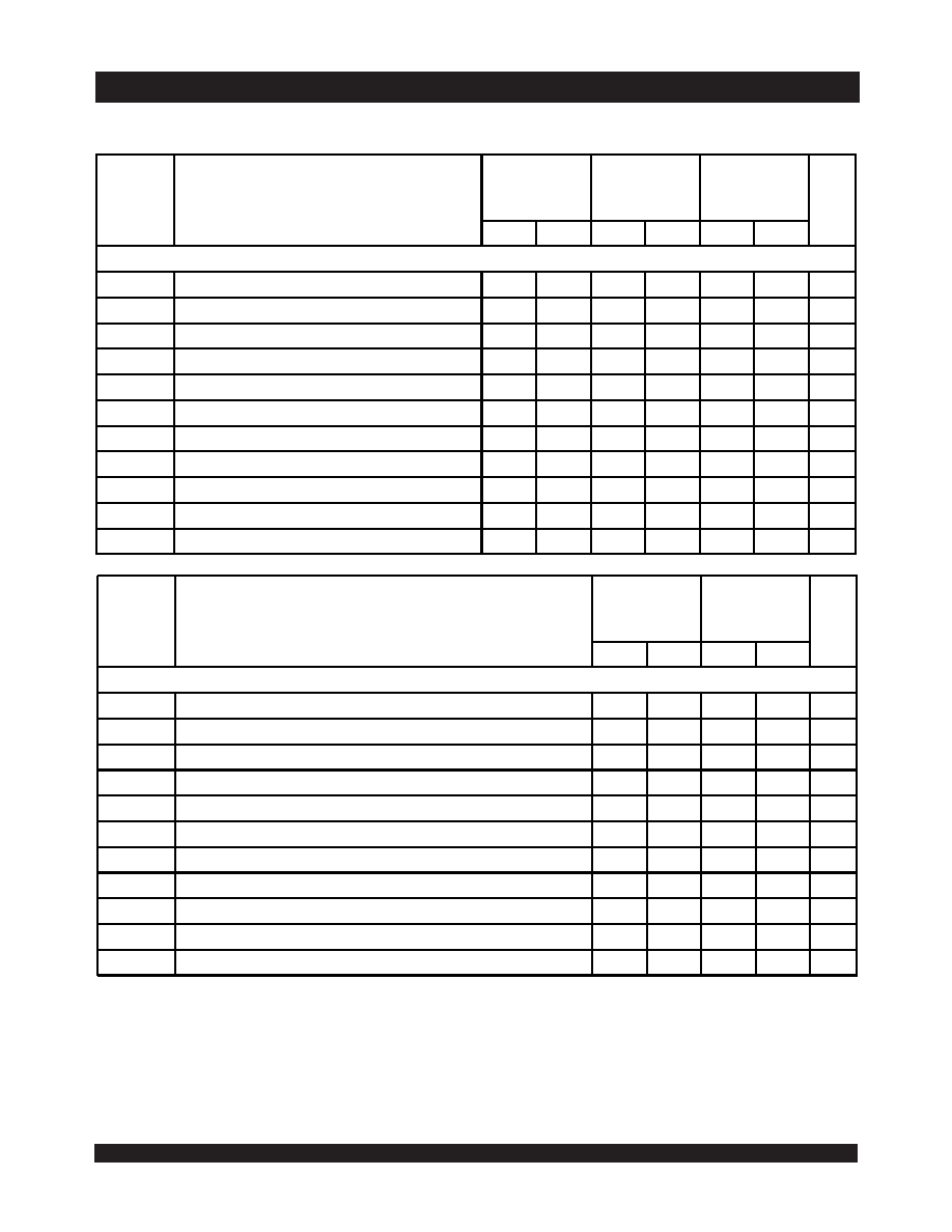
IDT7130SA/LA and IDT7140SA/LA
High-Speed 1K x 8 Dual-Port Static SRAM
Military, Industrial and Commercial Temperature Ranges
10
AC Electrical Characteristics Over the
Operating Temperature Supply Voltage Range(5)
NOTES:
1. Transition is measured 0mV from Low or High-impedance voltage with Output Test Load (Figure 2). This parameter is guaranteed by device characterization but
is not production tested.
2. PLCC, TQFP and STQFP packages only.
3. For MASTER/SLAVE combination, tWC = tBAA + tWP, since R/
W = VIL must occur after tBAA.
4. If
OE is LOW during a R/W controlled write cycle, the write pulse width must be the larger of tWP or (tWZ + tDW) to allow the I/O drivers to turn off data
to be placed on the bus for the required tDW. If
OE is HIGH during a R/W controlled write cycle, this requirement does not apply and the write pulse
can be as short as the specified tWP.
5. 'X' in part numbers indicates power rating (SA or LA).
Symbol
Parameter
7130X20
(2)
7140X20
(2)
Com'l Only
7130X25
7140X25
Com'l, Ind
& Military
7130X35
7140X35
Com'l
& Military
Unit
Min.
Max.
Min.
Max.
Min.
Max.
WRITE CYCLE
tWC
Write Cycle Time
(3)
20
____
25
____
35
____
ns
tEW
Chip Enable to End-of-Write
15
____
20
____
30
____
ns
tAW
Address Valid to End-of-Write
15
____
20
____
30
____
ns
tAS
Address Set-up Time
0
____
0
____
0
____
ns
tWP
Write Pulse Width
(4)
15
____
15
____
25
____
ns
tWR
Write Recovery Time
0
____
0
____
0
____
ns
tDW
Data Valid to End-of-Write
10
____
12
____
15
____
ns
tHZ
Output High-Z Time(1)
____
10
____
10
____
15
ns
tDH
Data Hold Time
0
____
0
____
0
____
ns
tWZ
Write Enable to Output in High-Z
(1)
____
10
____
10
____
15
ns
tOW
Output Active from End-of-Write
(1)
0
____
0
____
0
____
ns
2689 tbl 10a
Symbol
Parameter
7130X55
7140X55
Com'l, Ind
& Military
7130X100
7140X100
Com'l, Ind
& Military
Unit
Min.
Max.
Min.
Max.
WRITE CYCLE
tWC
Write Cycle Time
(3)
55
____
100
____
ns
tEW
Chip Enable to End-of-Write
40
____
90
____
ns
tAW
Address Valid to End-of-Write
40
____
90
____
ns
tAS
Address Set-up Time
0
____
0
____
ns
tWP
Write Pulse Width
(4)
30
____
55
____
ns
tWR
Write Recovery Time
0
____
0
____
ns
tDW
Data Valid to End-of-Write
20
____
40
____
ns
tHZ
Output High-Z Time(1)
____
25
____
40
ns
tDH
Data Hold Time
0
____
0
____
ns
tWZ
Write Enable to Output in High-Z
(1)
____
25
____
40
ns
tOW
Output Active from End-of-Write
(1)
0
____
0
____
ns
2689 tbl 10b
相关PDF资料 |
PDF描述 |
|---|---|
| 7140LA35CB | 1K X 8 DUAL-PORT SRAM, 35 ns, CDIP48 |
| 7134SA35PB | 4K X 8 DUAL-PORT SRAM, 35 ns, PDIP48 |
| 71522-1050 | 50 CONTACT(S), MALE, TELECOM AND DATACOM CONNECTOR, IDC, PLUG |
| 71522-2050 | 50 CONTACT(S), MALE, TELECOM AND DATACOM CONNECTOR, IDC, PLUG |
| 71522-3050 | 50 CONTACT(S), MALE, TELECOM AND DATACOM CONNECTOR, IDC, PLUG |
相关代理商/技术参数 |
参数描述 |
|---|---|
| 7130LA35TFG | 制造商:Integrated Device Technology Inc 功能描述:IC SRAM 8KBIT 35NS 64TQFP |
| 7130LA45TFI | 功能描述:IC SRAM 8KBIT 64TQFP 制造商:idt, integrated device technology inc 系列:* 零件状态:最後搶購 标准包装:160 |
| 7130LA45TFI8 | 功能描述:IC SRAM 8KBIT 64TQFP 制造商:idt, integrated device technology inc 系列:* 零件状态:最後搶購 标准包装:500 |
| 7130LA55C | 功能描述:静态随机存取存储器 RoHS:否 制造商:Cypress Semiconductor 存储容量:16 Mbit 组织:1 M x 16 访问时间:55 ns 电源电压-最大:3.6 V 电源电压-最小:2.2 V 最大工作电流:22 uA 最大工作温度:+ 85 C 最小工作温度:- 40 C 安装风格:SMD/SMT 封装 / 箱体:TSOP-48 封装:Tray |
| 7130LA55CB | 功能描述:静态随机存取存储器 RoHS:否 制造商:Cypress Semiconductor 存储容量:16 Mbit 组织:1 M x 16 访问时间:55 ns 电源电压-最大:3.6 V 电源电压-最小:2.2 V 最大工作电流:22 uA 最大工作温度:+ 85 C 最小工作温度:- 40 C 安装风格:SMD/SMT 封装 / 箱体:TSOP-48 封装:Tray |
发布紧急采购,3分钟左右您将得到回复。