- 您现在的位置:买卖IC网 > PDF目录234067 > 72805LB15PFI (INTEGRATED DEVICE TECHNOLOGY INC) 256 X 18 BI-DIRECTIONAL FIFO, 10 ns, PQFP128 PDF资料下载
参数资料
| 型号: | 72805LB15PFI |
| 厂商: | INTEGRATED DEVICE TECHNOLOGY INC |
| 元件分类: | FIFO |
| 英文描述: | 256 X 18 BI-DIRECTIONAL FIFO, 10 ns, PQFP128 |
| 封装: | TQFP-128 |
| 文件页数: | 18/26页 |
| 文件大小: | 336K |
| 代理商: | 72805LB15PFI |
25
COMMERCIAL AND INDUSTRIAL
TEMPERATURE RANGES
IDT72805LB/72815LB/72825LB/72835LB/72845LB CMOS Dual SyncFIFOTM
256 x 18, 512 x 18, 1,024 x 18, 2,048 x 18 and 4,096 x 18
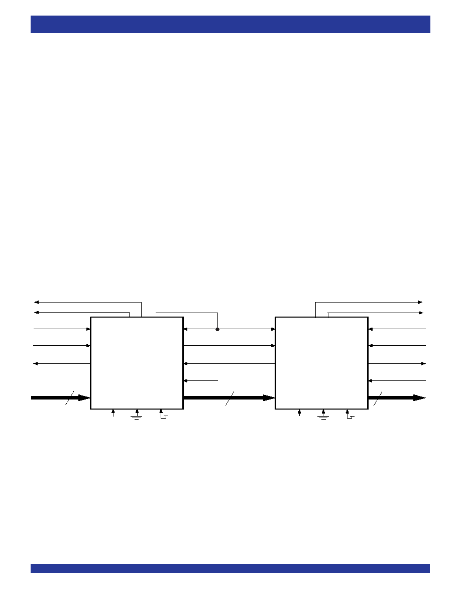
Figure 31. Block Diagram of 512 x 18, 1,024 x 18, 2,048 x 18, 4,096 x 18, 8,192 x 18 Synchronous
FIFO Memory With Programmable Flags used in Depth Expansion Configuration
Dn
INPUT READY
WRITE ENABLE
WRITE CLOCK
WEN
WCLK
IR
DATA IN
RCLK
READ CLOCK
RCLK
REN
OE
OUTPUT ENABLE
OUTPUT READY
Qn
Dn
IR
GND
WEN
WCLK
OR
REN
OE
Qn
READ ENABLE
OR
DATA OUT
TRANSFER CLOCK
3139 drw 31
n
RXI
HF
72805
72815
72825
72835
72845
WXI
FL
VCC
GND
(0,1)
72805
72815
72825
72835
72845
RXI
WXI
FL
VCC
GND
(0,1)
PAF
HF
PAE
DEPTH EXPANSION CONFIGURATION (FWFT MODE)
In FWFT mode, the FIFOs can be connected in series (the data outputs
of one FIFO connected to the data inputs of the next) with no external logic
necessary. The resulting configuration provides a total depth equivalent to
the sum of the depths associated with each single FIFO. Figure 31 shows
a depth expansion using one IDT72805LB/72815LB/72825LB/72835LB/
72845LB devices.
Care should be taken to select FWFT mode during Master Reset for all
FIFOs in the depth expansion configuration. The first word written to an
empty configuration will pass from one FIFO to the next (“ripple down”) until
it finally appears at the outputs of the last FIFO in the chain–no read
operation is necessary but the RCLK of each FIFO must be free-running.
Each time the data word appears at the outputs of one FIFO, that device’s
OR line goes LOW, enabling a write to the next FIFO in line.
For an empty expansion configuration, the amount of time it takes for
OR
of the last FIFO in the chain to go LOW (i.e. valid data to appear on the last
FIFO’s outputs) after a word has been written to the first FIFO is the sum of
the delays for each individual FIFO:
(N – 1)*(4*transfer clock) + 3*TRCLK
where N is the number of FIFOs in the expansion and TRCLK is the RCLK
period. Note that extra cycles should be added for the possibility that the
tSKEW1 specification is not met between WCLK and transfer clock, or RCLK
and transfer clock, for the
OR flag.
The “ripple down” delay is only noticeable for the first word written to an
empty depth expansion configuration. There will be no delay evident for
subsequent words written to the configuration.
The first free location created by reading from a full depth expansion
configuration will “bubble up” from the last FIFO to the previous one until it
finally moves into the first FIFO of the chain. Each time a free location is
created in one FIFO of the chain, that FIFO’s
IR line goes LOW, enabling
the preceding FIFO to write a word to fill it.
For a full expansion configuration, the amount of time it takes for
IR of the
first FIFO in the chain to go LOW after a word has been read from the last
FIFO is the sum of the delays for each individual FIFO:
(N – 1)*(3*transfer clock) + 2 TWCLK
where N is the number of FIFOs in the expansion and TWCLK is the WCLK
period. Note that extra cycles should be added for the possibility that the
tSKEW1 specification is not met between RCLK and transfer clock, or WCLK
and transfer clock, for the
IR flag.
The Transfer Clock line should be tied to either WCLK or RCLK,
whichever is faster. Both these actions result in data moving, as quickly as
possible, to the end of the chain and free locations to the beginning of the
chain.
相关PDF资料 |
PDF描述 |
|---|---|
| 7R8FLE232I25 | 4M X 16 FLASH 5V PROM CARD, 150 ns, UUC68 |
| 70V658S10BC | 64K X 36 DUAL-PORT SRAM, 10 ns, PBGA256 |
| 7R32FLE211I15 | 16M X 16 FLASH 5V PROM CARD, 150 ns, UUC68 |
| 7R8FLE220C15 | 4M X 16 FLASH 5V PROM CARD, 150 ns, UUC68 |
| 7R8FLE242C25 | 4M X 16 FLASH 5V PROM CARD, 150 ns, UUC68 |
相关代理商/技术参数 |
参数描述 |
|---|---|
| 72805LB15PFI8 | 制造商:Integrated Device Technology Inc 功能描述:FIFO Mem Sync Quad Depth/Width Bi-Dir 256 x 18 x 2 128-Pin TQFP T/R 制造商:Integrated Device Technology Inc 功能描述:FIFO SYNC QUAD DEPTH/WIDTH BI-DIR 256 X 18 X 2 128TQFP - Tape and Reel |
| 72805LB25BG | 制造商:Integrated Device Technology Inc 功能描述:FIFO Mem Sync Quad Depth/Width Bi-Dir 256 x 18 x 2 121-Pin BGA 制造商:Integrated Device Technology Inc 功能描述:FIFO SYNC QUAD DEPTH/WIDTH BI-DIR 256 X 18 X 2 121BGA - Rail/Tube |
| 72805LB25BG8 | 制造商:Integrated Device Technology Inc 功能描述:FIFO Mem Sync Quad Depth/Width Bi-Dir 256 x 18 x 2 121-Pin BGA T/R 制造商:Integrated Device Technology Inc 功能描述:FIFO SYNC QUAD DEPTH/WIDTH BI-DIR 256 X 18 X 2 121BGA - Tape and Reel |
| 72805LB25PF | 功能描述:先进先出 RoHS:否 制造商:IDT 电路数量: 数据总线宽度:18 bit 总线定向:Unidirectional 存储容量:4 Mbit 定时类型:Synchronous 组织:256 K x 18 最大时钟频率:100 MHz 访问时间:10 ns 电源电压-最大:3.6 V 电源电压-最小:6 V 最大工作电流:35 mA 最大工作温度:+ 85 C 封装 / 箱体:TQFP-80 封装: |
| 72805LB25PF8 | 功能描述:先进先出 RoHS:否 制造商:IDT 电路数量: 数据总线宽度:18 bit 总线定向:Unidirectional 存储容量:4 Mbit 定时类型:Synchronous 组织:256 K x 18 最大时钟频率:100 MHz 访问时间:10 ns 电源电压-最大:3.6 V 电源电压-最小:6 V 最大工作电流:35 mA 最大工作温度:+ 85 C 封装 / 箱体:TQFP-80 封装: |
发布紧急采购,3分钟左右您将得到回复。