- 您现在的位置:买卖IC网 > PDF目录298505 > 72841L10PF (INTEGRATED DEVICE TECHNOLOGY INC) 4K X 9 BI-DIRECTIONAL FIFO, 6.5 ns, PQFP64 PDF资料下载
参数资料
| 型号: | 72841L10PF |
| 厂商: | INTEGRATED DEVICE TECHNOLOGY INC |
| 元件分类: | FIFO |
| 英文描述: | 4K X 9 BI-DIRECTIONAL FIFO, 6.5 ns, PQFP64 |
| 封装: | TQFP-64 |
| 文件页数: | 10/16页 |
| 文件大小: | 211K |
| 代理商: | 72841L10PF |
3
IDT72801/728211/72821/72831/72841/72851 DUAL CMOS SyncFIFOTM
DUAL 256 x 9, DUAL 512 x 9, DUAL 1K x 9, DUAL 2K x 9, DUAL 4K x 9, DUAL 8K x 9
COMMERCIAL AND INDUSTRIAL
TEMPERATURERANGES
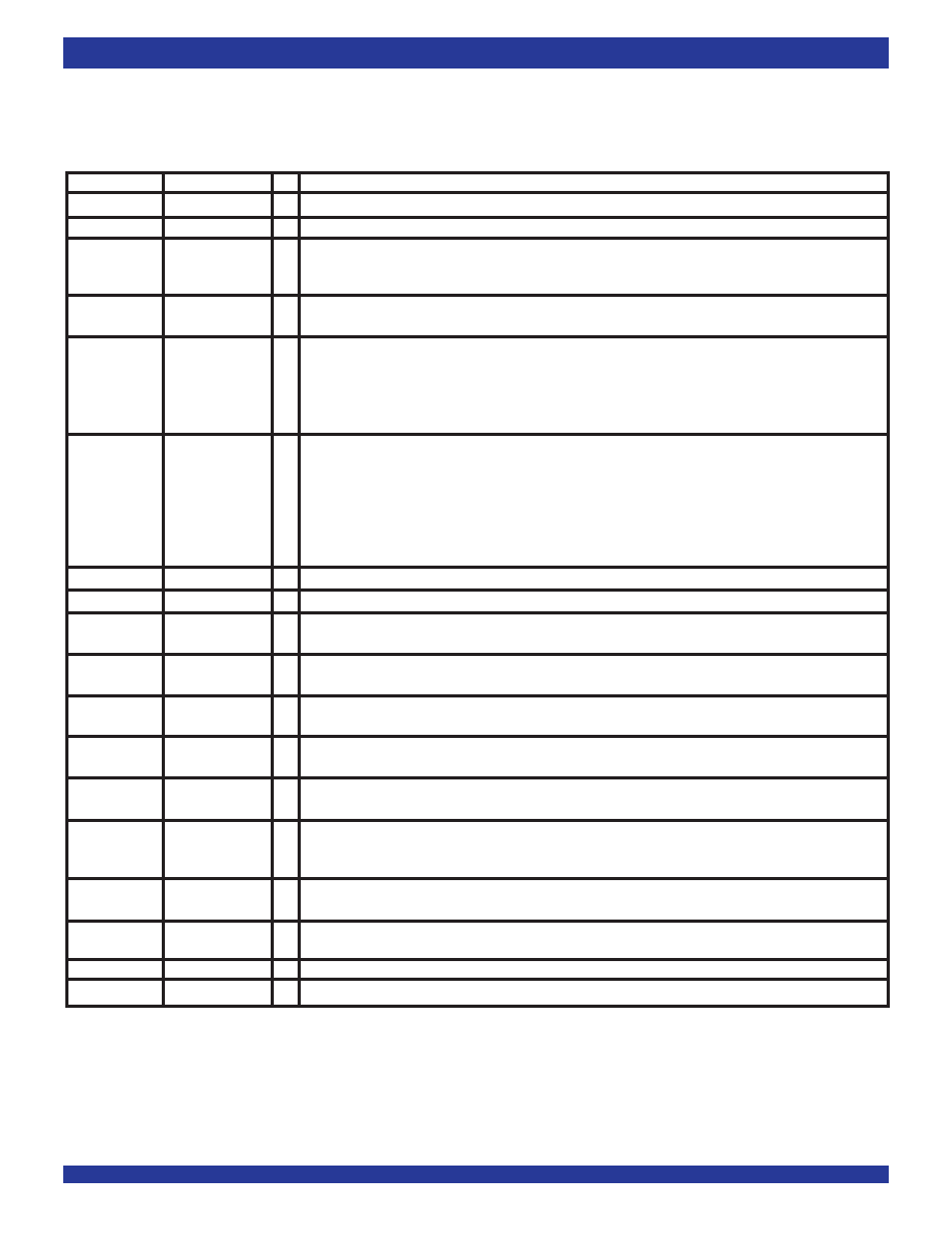
Symbol
Name
I/O
Description
DA0-DA8
A Data Inputs
I
9-bit data inputs to RAM array A.
DB0-DB8
B Data Inputs
I
9-bit data inputs to RAM array B.
RSA, RSB
Reset
I
When RSA (RSB) is set LOW, the associated internal read and write pointers of array A (B) are set to
the first location; FFA (FFB) and PAFA (PAFB) go HIGH, and PAEA (PAEB) and EFA (EFB) go
LOW. After power-up, a reset of both FIFOs A and B is required before an initial Write.
WCLKA
WriteClock
I
Data is written into the FIFO A (B) on a LOW-to-HIGH transition of WCLKA (WCLKB) when the write
WCLKB
enable(s) are asserted.
WENA1
Write Enable 1
I
If FIFO A (B) is configured to have programmable flags, WENA1 (WENB1) is the only Write
WENB1
Enable pin that can be used. When WENA1 (WENB1) is LOW, data A (B) is written into the FIFO
on every LOW-to-HIGH transition WCLKA (WCLKB). If the FIFO is configured to have two write enables,
WENA1 (WENB1) must be LOW and WENA2 (WENB2) must be HIGH to write data into the FIFO. Data
will not be written into the FIFO if FFA (FFB) is LOW.
WENA2/LDA
Write Enable 2/
I
FIFO A (B) is configured at reset to have either two write enables or programmable flags. If LDA (LDB)
WENB2/LDB
Load
is HIGH at reset, this pin operates as a second write enable. If WENA2/LDA (WENB2/LDB) is LOW
at reset this pin operates as a control to load and read the programmable flag offsets for its respective array.
If the FIFO is configured to have two write enables, WENA1 (WENB1) must be LOW
and WENA2 (WENB2) must be HIGH to write data into FIFO A (B). Data will not be written into FIFO A (B)
if FFA (FFB) is LOW. If the FIFO is configured to have programmable flags, LDA
(LDB) is held
LOW to write or read the programmable flag offsets.
QA0-QA8
A Data Outputs
O
9-bit data outputs from RAM array A.
QB0-QB8
B Data Outputs
O
9-bit data outputs from RAM array B.
RCLKA
Read Clock
I
Data is read from FIFO A (B) on a LOW-to-HIGH transition of RCLKA (RCLKB) when RENA1
RCLKB
(RENB1) and RENA2 (RENB2) are asserted.
RENA1
Read Enable 1
I
When RENA1 (RENB1) and RENA2 (RENB2) are LOW, data is read from FIFO A (B) on every
RENB1
LOW-to-HIGH transition of RCLKA (RCLKB). Data will not be read from Array A (B) if EFA (EFB) is LOW.
RENA2
Read Enable 2
I
When RENA1 (RENB1) and RENA2 (RENB2) are LOW, data is read from the FIFO A (B) on every
RENB2
LOW-to-HIGH transition of RCLKA (RCLKB). Data will not be read from array A (B) if the EFA (EFB) is LOW.
OEA
OutputEnable
I
When OEA (OEB) is LOW, outputs DA0-DA8 (DB0-DB8) are active. If OEA (OEB) is HIGH, the
OEB
outputs DA0-DA8 (DB0-DB8) will be in a high-impedance state.
EFA
Empty Flag
O
When EFA (EFB) is LOW, FIFO A (B) is empty and further data reads from the output are inhibited.
EFB
When EFA (EFB) is HIGH, FIFO A (B) is not empty. EFA (EFB) is synchronized to RCLKA (RCLKB).
PAEA
Programmable
O
When PAEA (PAEB) is LOW, FIFO A (B) is almost-empty based on the offset programmed into the
PAEB
Almost-Empty
appropriate offset register. The default offset at reset is Empty+7. PAEA (PAEB) is synchronized to
Flag
RCLKA (RCLKB).
PAFA
Programmable
O
When PAFA (PAFB) is LOW, FIFO A (B) is almost-full based on the offset programmed into the appropriate
PAFB
Almost-FullFlag
offset register. The default offset at reset is Full-7. PAFA (PAFB) is synchronized to WCLKA (WCLKB).
FFA
Full Flag
O
When FFA (FFB) is LOW, FIFO A (B) is full and further data writes into the input are inhibited.
FFB
When FFA (FFB) is HIGH, FIFO A (B) is not full. FFA (FFB) is synchronized to WCLKA (WCLKB).
VCC
Power
+5V power supply pin.
GND
Ground
0V ground pin.
PIN DESCRIPTIONS
The IDT72801/72811/72821/72831/72841/72851s two FIFOs, referred
to as FIFO A and FIFO B, are identical in every respect. The following
description defines the input and output signals for FIFO A. The correspond-
ing signal names for FIFO B are provided in parentheses.
相关PDF资料 |
PDF描述 |
|---|---|
| 72821L15TF8 | 1K X 9 BI-DIRECTIONAL FIFO, 10 ns, PQFP64 |
| 72R99-P | 25 A, BARRIER STRIP TERMINAL BLOCK, 1 ROW, 1 DECK |
| 72R99-M | 25 A, BARRIER STRIP TERMINAL BLOCK, 1 ROW, 1 DECK |
| 72R99-59 | 25 A, BARRIER STRIP TERMINAL BLOCK, 1 ROW, 1 DECK |
| 72R99-49 | 25 A, BARRIER STRIP TERMINAL BLOCK, 1 ROW, 1 DECK |
相关代理商/技术参数 |
参数描述 |
|---|---|
| 72841L10PF8 | 功能描述:先进先出 RoHS:否 制造商:IDT 电路数量: 数据总线宽度:18 bit 总线定向:Unidirectional 存储容量:4 Mbit 定时类型:Synchronous 组织:256 K x 18 最大时钟频率:100 MHz 访问时间:10 ns 电源电压-最大:3.6 V 电源电压-最小:6 V 最大工作电流:35 mA 最大工作温度:+ 85 C 封装 / 箱体:TQFP-80 封装: |
| 72841L10PFG | 功能描述:先进先出 RoHS:否 制造商:IDT 电路数量: 数据总线宽度:18 bit 总线定向:Unidirectional 存储容量:4 Mbit 定时类型:Synchronous 组织:256 K x 18 最大时钟频率:100 MHz 访问时间:10 ns 电源电压-最大:3.6 V 电源电压-最小:6 V 最大工作电流:35 mA 最大工作温度:+ 85 C 封装 / 箱体:TQFP-80 封装: |
| 72841L10PFG8 | 制造商:Integrated Device Technology Inc 功能描述:FIFO Mem Sync Quad Depth/Width Bi-Dir 4K x 9 x 2 64-Pin TQFP T/R 制造商:Integrated Device Technology Inc 功能描述:FIFO SYNC QUAD DEPTH/WIDTH BI-DIR 4KX9X2 64TQFP - Tape and Reel |
| 72841L10TF | 功能描述:先进先出 RoHS:否 制造商:IDT 电路数量: 数据总线宽度:18 bit 总线定向:Unidirectional 存储容量:4 Mbit 定时类型:Synchronous 组织:256 K x 18 最大时钟频率:100 MHz 访问时间:10 ns 电源电压-最大:3.6 V 电源电压-最小:6 V 最大工作电流:35 mA 最大工作温度:+ 85 C 封装 / 箱体:TQFP-80 封装: |
| 72841L10TF8 | 制造商:Integrated Device Technology Inc 功能描述:FIFO Mem Sync Quad Depth/Width Bi-Dir 4K x 9 x 2 64-Pin STQFP T/R 制造商:Integrated Device Technology Inc 功能描述:FIFO SYNC QUAD DEPTH/WIDTH BI-DIR 4KX9X2 64TQFP - Tape and Reel |
发布紧急采购,3分钟左右您将得到回复。