- 您现在的位置:买卖IC网 > PDF目录8030 > 74ABT544D,602 (NXP Semiconductors)IC TRANSCVR 3-ST 8BIT INV 24SOIC PDF资料下载
参数资料
| 型号: | 74ABT544D,602 |
| 厂商: | NXP Semiconductors |
| 文件页数: | 13/16页 |
| 文件大小: | 0K |
| 描述: | IC TRANSCVR 3-ST 8BIT INV 24SOIC |
| 标准包装: | 30 |
| 系列: | 74ABT |
| 逻辑类型: | 收发器,反相 |
| 元件数: | 1 |
| 每个元件的位元数: | 8 |
| 输出电流高,低: | 32mA,64mA |
| 电源电压: | 4.5 V ~ 5.5 V |
| 工作温度: | -40°C ~ 85°C |
| 安装类型: | 表面贴装 |
| 封装/外壳: | 24-SOIC(0.295",7.50mm 宽) |
| 供应商设备封装: | 24-SO |
| 包装: | 管件 |
| 其它名称: | 568-2485-5 935047950602 |
74ABT544
All information provided in this document is subject to legal disclaimers.
NXP B.V. 2011. All rights reserved.
Product data sheet
Rev. 6 — 3 November 2011
6 of 16
NXP Semiconductors
74ABT544
Octal latched transceiver with dual enable; 3-state
[1]
For valid test results, data must not be loaded into the flip-flops (or latches) after applying the power.
[2]
This parameter is valid for any VCC between 0 V and 2.1 V, with a transition time of up to 10 ms. From VCC = 2.1 V to VCC = 5 V 10 %,
a transition time of up to 100
s is permitted.
[3]
Not more than one output should be tested at a time, and the duration of the test should not exceed one second.
[4]
This is the increase in supply current for each input at 3.4 V.
10. Dynamic characteristics
VOL(pu)
power-up LOW-level
output voltage
VCC = 5.5 V; IO =1mA;
VI =GND or VCC
-
0.13
0.55
-
0.55
V
II
input leakage current
VCC = 5.5 V; VI =GND or 5.5V
control pins
-
0.01 1.0
-
1.0
A
An, Bn
-
5.0 100
-
100
A
IOFF
power-off leakage
current
VCC = 0 V; VI or VO 4.5 V
-
5.0 100
-
100
A
IO(pu/pd)
power-up/power-down
output current
VCC = 2.1 V; VO =0.5 V;
VI =GND or VCC;
OEAB,OEBA don’t care
-
5.0
50
-
50
A
IOZ
OFF-state output
current
VCC = 5.5 V; VI = VIL or VIH
VO = 2.7 V
-
5.0
50
-
50
A
VO = 0.5 V
-
5.0
50
-
50
A
ILO
output leakage current HIGH-state; VO =5.5 V;
VCC =5.5 V; VI =GND or VCC
-5.0
50
-
50
A
IO
output current
VCC = 5.5 V; VO = 2.5 V
180
65
50
180
50
mA
ICC
supply current
VCC = 5.5 V; VI = GND or VCC
outputs HIGH-state
-
110
250
-
250
A
outputs LOW-state
-
20
30
-
30
mA
outputs disabled
-
110
250
-
250
A
I
CC
additional supply
current
per input pin; VCC = 5.5 V; one input
pin at 3.4 V, other inputs at VCC or
GND
-
0.3
1.5
-
1.5
mA
CI
input capacitance
VI = 0 V or VCC
-4-
-
pF
CI/O
input/output
capacitance
outputs disabled; VO =0 V or VCC
-7-
-
pF
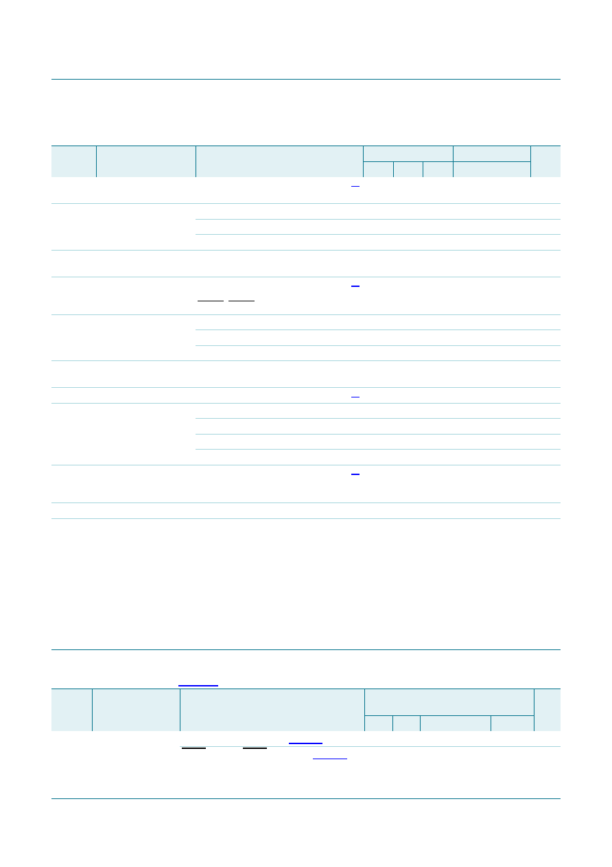
Table 6.
Static characteristics …continued
Voltages are referenced to GND (ground = 0 V).
Symbol
Parameter
Conditions
25
C
40 C to +85 C Unit
Min
Typ
Max
Min
Max
Table 7.
Dynamic characteristics
GND = 0 V; for test circuit, see Figure 10.
Symbol Parameter
Conditions
25
C; V
CC = 5.0 V
40 C to +85 C;
VCC = 5.0 V 0.5 V
Unit
Min
Typ
Max
Min
Max
tPLH
LOW to HIGH
propagation delay
An to Bn or Bn to An; see Figure 5
1.7
3.0
3.8
1.7
4.7
ns
LEBA to An or LEAB to Bn; see Figure 6
2.1
3.5
4.2
2.1
5.2
ns
相关PDF资料 |
PDF描述 |
|---|---|
| OSTHN185052 | CON TERM BLOCK 18POS 5.08MM |
| OSTVD223152 | TERM BLOCK PLUG 3.81MM 22POS |
| EDZ1100/11 | TERM BLOCK PLUG 5.08MM 11POS |
| SY100E337JZ | IC TXRX BUS 3BIT SCAM REG 28PLCC |
| EDSTLZ976/5 | TERM BLOCK HDR 5.08MM 5POS PCB |
相关代理商/技术参数 |
参数描述 |
|---|---|
| 74ABT544DB | 功能描述:总线收发器 OCTAL LATCHED XCVR INV 3-S RoHS:否 制造商:Fairchild Semiconductor 逻辑类型:CMOS 逻辑系列:74VCX 每芯片的通道数量:16 输入电平:CMOS 输出电平:CMOS 输出类型:3-State 高电平输出电流:- 24 mA 低电平输出电流:24 mA 传播延迟时间:6.2 ns 电源电压-最大:2.7 V, 3.6 V 电源电压-最小:1.65 V, 2.3 V 最大工作温度:+ 85 C 封装 / 箱体:TSSOP-48 封装:Reel |
| 74ABT544DB,112 | 功能描述:总线收发器 OCTAL LATCHED XCVR RoHS:否 制造商:Fairchild Semiconductor 逻辑类型:CMOS 逻辑系列:74VCX 每芯片的通道数量:16 输入电平:CMOS 输出电平:CMOS 输出类型:3-State 高电平输出电流:- 24 mA 低电平输出电流:24 mA 传播延迟时间:6.2 ns 电源电压-最大:2.7 V, 3.6 V 电源电压-最小:1.65 V, 2.3 V 最大工作温度:+ 85 C 封装 / 箱体:TSSOP-48 封装:Reel |
| 74ABT544DB,118 | 功能描述:总线收发器 OCTAL LATCHED XCVR RoHS:否 制造商:Fairchild Semiconductor 逻辑类型:CMOS 逻辑系列:74VCX 每芯片的通道数量:16 输入电平:CMOS 输出电平:CMOS 输出类型:3-State 高电平输出电流:- 24 mA 低电平输出电流:24 mA 传播延迟时间:6.2 ns 电源电压-最大:2.7 V, 3.6 V 电源电压-最小:1.65 V, 2.3 V 最大工作温度:+ 85 C 封装 / 箱体:TSSOP-48 封装:Reel |
| 74ABT544DB-T | 功能描述:总线收发器 OCTAL LATCHED XCVR INV 3-S RoHS:否 制造商:Fairchild Semiconductor 逻辑类型:CMOS 逻辑系列:74VCX 每芯片的通道数量:16 输入电平:CMOS 输出电平:CMOS 输出类型:3-State 高电平输出电流:- 24 mA 低电平输出电流:24 mA 传播延迟时间:6.2 ns 电源电压-最大:2.7 V, 3.6 V 电源电压-最小:1.65 V, 2.3 V 最大工作温度:+ 85 C 封装 / 箱体:TSSOP-48 封装:Reel |
| 74ABT544D-T | 功能描述:总线收发器 OCTAL LATCHED XCVR INV 3-S RoHS:否 制造商:Fairchild Semiconductor 逻辑类型:CMOS 逻辑系列:74VCX 每芯片的通道数量:16 输入电平:CMOS 输出电平:CMOS 输出类型:3-State 高电平输出电流:- 24 mA 低电平输出电流:24 mA 传播延迟时间:6.2 ns 电源电压-最大:2.7 V, 3.6 V 电源电压-最小:1.65 V, 2.3 V 最大工作温度:+ 85 C 封装 / 箱体:TSSOP-48 封装:Reel |
发布紧急采购,3分钟左右您将得到回复。