- 您现在的位置:买卖IC网 > PDF目录360407 > 74AHCT74 (NXP Semiconductors N.V.) Dual D-type flip-flop with set and reset; positive-edge trigger(带置位和复位的双D触发器;上升沿触发;) PDF资料下载
参数资料
| 型号: | 74AHCT74 |
| 厂商: | NXP Semiconductors N.V. |
| 英文描述: | Dual D-type flip-flop with set and reset; positive-edge trigger(带置位和复位的双D触发器;上升沿触发;) |
| 中文描述: | 双D型触发器设置和复位触发器,积极边缘触发器(带置位和复位的双?触发器,上升沿触发;) |
| 文件页数: | 2/20页 |
| 文件大小: | 92K |
| 代理商: | 74AHCT74 |
1999 Sep 23
2
Philips Semiconductors
Product specification
Dual D-type flip-flop with set and reset;
positive-edge trigger
74AHC74; 74AHCT74
FEATURES
ESD protection:
HBM EIA/JESD22-A114-A
exceeds 2000 V
MM EIA/JESD22-A115-A
exceeds 200 V
Balanced propagation delays
Inputsacceptsvoltageshigherthan
V
CC
For AHC only:
operates with CMOS input levels
For AHCT only:
operates with TTL input levels
Output capability: standard
I
CC
category: flip-flops
Specified from
40 to +85 and +125
°
C.
DESCRIPTION
The 74AHC/AHCT74 are high-speed
Si-gate CMOS devices and are pin
compatible with low power Schottky
TTL (LSTTL). They are specified in
compliance with JEDEC standard
No. 7A.
The 74AHC/AHCT74 dual
positive-edge triggered, D-type
flip-flops with individual data (D)
inputs,clock (CP)inputs,set (S
D
)and
reset (R
D
) inputs; also
complementary Q and Q outputs.
The set and reset are asynchronous
active LOW inputs and operate
independently of the clock input.
Information on the data input is
transferred to the Q output on the
LOW-to-HIGH transition of the clock
pulse. The D inputs must be stable
one set-up time prior to the
LOW-to-HIGH clock transition for
predictable operation.
Schmitt-trigger action in the clock
input makes the circuit highly tolerant
to slower clock rise and fall times.
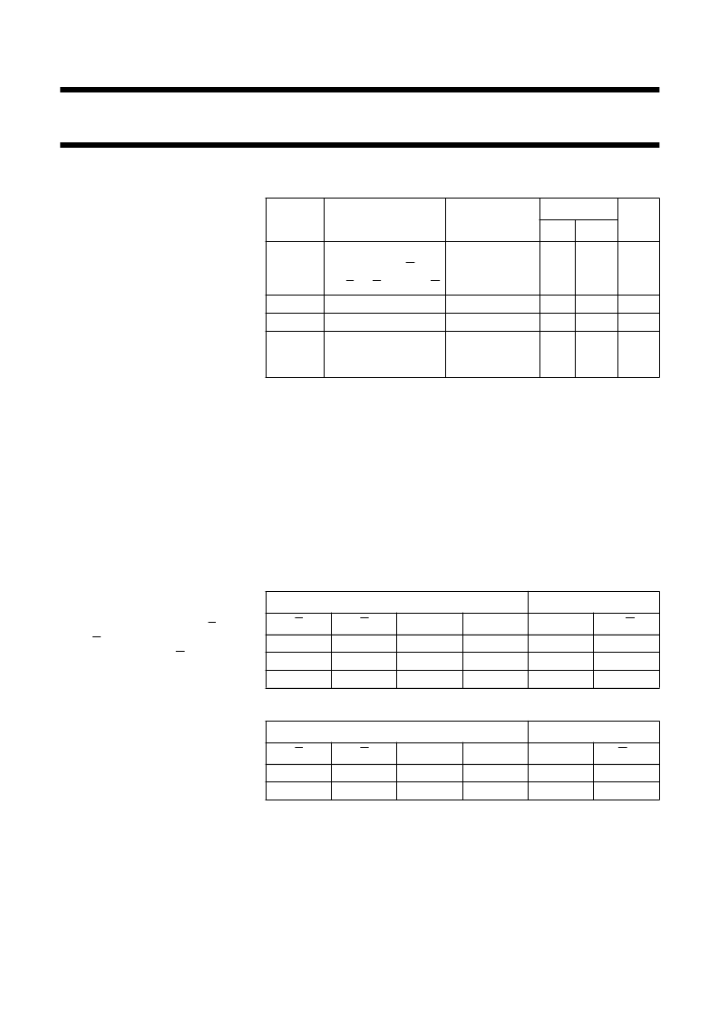
QUICK REFERENCE DATA
GND = 0 V; T
amb
= 25
°
C; t
r
= t
f
≤
3.0 ns.
Notes
1.
C
PD
is used to determine the dynamic power dissipation (P
D
in
μ
W).
P
D
= C
PD
×
V
CC2
×
f
i
+
∑
(C
L
×
V
CC2
×
f
o
) where:
f
i
= input frequency in MHz; f
o
= output frequency in MHz;
∑
(C
L
×
V
CC2
×
f
o
) = sum of outputs;
C
L
= output load capacitance in pF;
V
CC
= supply voltage in Volts.
The condition is V
I
= GND to V
CC
.
2.
FUNCTION TABLES
Table 1
See note 1
Table 2
See note 1
Note to Tables 1 and 2
1.
H = HIGH voltage level;
L = LOW voltage level;
X = don’t care;
↑
= LOW-to-HIGH CP transition;
Q
n+1
= state after the next LOW-to-HIGH CP transition.
SYMBOL
PARAMETER
CONDITIONS
TYPICAL
UNIT
AHC
AHCT
t
PHL
/t
PLH
propagation delay
nCP to nQ, nQ
nS
D
, nR
D
to nQ, nQ
max. clock frequency
input capacitance
power dissipation
capacitance
C
L
= 15 pF;
V
CC
= 5 V
3.7
3.7
130
3.3
3.7
100
4.0
16
ns
ns
MHz
pF
pF
f
max
C
I
C
PD
V
I
= V
CC
or GND 4.0
C
L
= 50 pF;
f = 1 MHz;
notes 1 and 2
12
INPUT
OUTPUT
nS
D
L
H
L
nR
D
H
L
L
nCP
nD
nQ
nQ
X
X
X
X
X
X
H
L
H
L
H
H
INPUT
OUTPUT
nS
D
H
H
nR
D
H
H
nCP
↑
↑
nD
nQ
n+1
L
H
nQ
n+1
H
L
L
H
相关PDF资料 |
PDF描述 |
|---|---|
| 74AHC86 | Quad 2-input EXCLUSIVE-OR gate(四2输入异或门) |
| 74AHCT86 | Quad 2-input EXCLUSIVE-OR gate(四2输入异或门) |
| 74AHC86PWDH | Quadruple 2-Input Positive-NAND Gates With Open-Drain Outputs 14-TSSOP -40 to 85 |
| 74AHCT86PWDH | Triple 3-Input Positive-NAND Gates 14-SOIC -40 to 85 |
| 74AHCT00 | Quad 2-input NAND gate(四 2输入与非门) |
相关代理商/技术参数 |
参数描述 |
|---|---|
| 74AHCT74BQ | 制造商:NXP Semiconductors 功能描述:IC DUAL D F-F POS EDGE DHVQ |
| 74AHCT74BQ,115 | 功能描述:触发器 DUAL D-TYPE FLIPFLOP RoHS:否 制造商:Texas Instruments 电路数量:2 逻辑系列:SN74 逻辑类型:D-Type Flip-Flop 极性:Inverting, Non-Inverting 输入类型:CMOS 输出类型: 传播延迟时间:4.4 ns 高电平输出电流:- 16 mA 低电平输出电流:16 mA 电源电压-最大:5.5 V 最大工作温度:+ 85 C 安装风格:SMD/SMT 封装 / 箱体:X2SON-8 封装:Reel |
| 74AHCT74BQ-G | 功能描述:触发器 DUAL D-TYPE FLIPFLOP RoHS:否 制造商:Texas Instruments 电路数量:2 逻辑系列:SN74 逻辑类型:D-Type Flip-Flop 极性:Inverting, Non-Inverting 输入类型:CMOS 输出类型: 传播延迟时间:4.4 ns 高电平输出电流:- 16 mA 低电平输出电流:16 mA 电源电压-最大:5.5 V 最大工作温度:+ 85 C 安装风格:SMD/SMT 封装 / 箱体:X2SON-8 封装:Reel |
| 74AHCT74BQ-Q100X | 制造商:NXP Semiconductors 功能描述:74AHCT74BQ-Q100/DHVQFN14/REEL7 - Tape and Reel 制造商:NXP Semiconductors 功能描述:IC D-TYPE POS TRG DUAL 14DHVQFN |
| 74AHCT74D | 功能描述:触发器 DUAL D-TYPE FLIPFLOP RoHS:否 制造商:Texas Instruments 电路数量:2 逻辑系列:SN74 逻辑类型:D-Type Flip-Flop 极性:Inverting, Non-Inverting 输入类型:CMOS 输出类型: 传播延迟时间:4.4 ns 高电平输出电流:- 16 mA 低电平输出电流:16 mA 电源电压-最大:5.5 V 最大工作温度:+ 85 C 安装风格:SMD/SMT 封装 / 箱体:X2SON-8 封装:Reel |
发布紧急采购,3分钟左右您将得到回复。