- 您现在的位置:买卖IC网 > PDF目录360409 > 74ALS109A (NXP Semiconductors N.V.) Dual J-K positive edge-triggered flip-flop with set and reset PDF资料下载
参数资料
| 型号: | 74ALS109A |
| 厂商: | NXP Semiconductors N.V. |
| 英文描述: | Dual J-K positive edge-triggered flip-flop with set and reset |
| 中文描述: | 双JK上升沿触发器设置和复位触发器 |
| 文件页数: | 2/9页 |
| 文件大小: | 93K |
| 代理商: | 74ALS109A |
Philips Semiconductors
Product specification
74ALS109A
Dual J-K positive edge triggered flip-flop
with set and reset
2
1991 Feb 08
853–1275 01670
DESCRIPTION
The 74ALS109A is a dual positive edge-triggered JK-type flip-flop
featuring individual J, K, clock, set, and reset inputs; also true and
complementary outputs. Set (SD) and reset (RD) are asynchronous
active-Low inputs and operate independently of the clock (CP) input.
The J and K are edge-triggered inputs which control the state
changes of the flip-flops as described in the function table. Clock
triggering occurs at a voltage level and is not directly related to the
transition time of the positive-going pulse. The J and K inputs must
be stable just one setup time prior to the Low-to-High transition of
the clock for predictable operation. The JK design allows operation
as a D flip-flop by tying J and K inputs together. Although the clock
input is level sensitive, the positive transition of the clock pulse
between the 0.8V and 2.0V levels should be equal to or less than
the clock to output delay time for reliable operation.
TYPE
TYPICAL
f
MAX
TYPICAL
SUPPLY CURRENT
(TOTAL)
74ALS109A
150MHz
3.0mA
ORDERING INFORMATION
ORDER CODE
DESCRIPTION
COMMERCIAL RANGE
V
CC
= 5V
±
10%,
T
amb
= 0
°
C to +70
°
C
DRAWING
NUMBER
16-pin plastic DIP
74ALS109AN
SOT38-4
16-pin plastic SO
74ALS109AD
SOT109-1
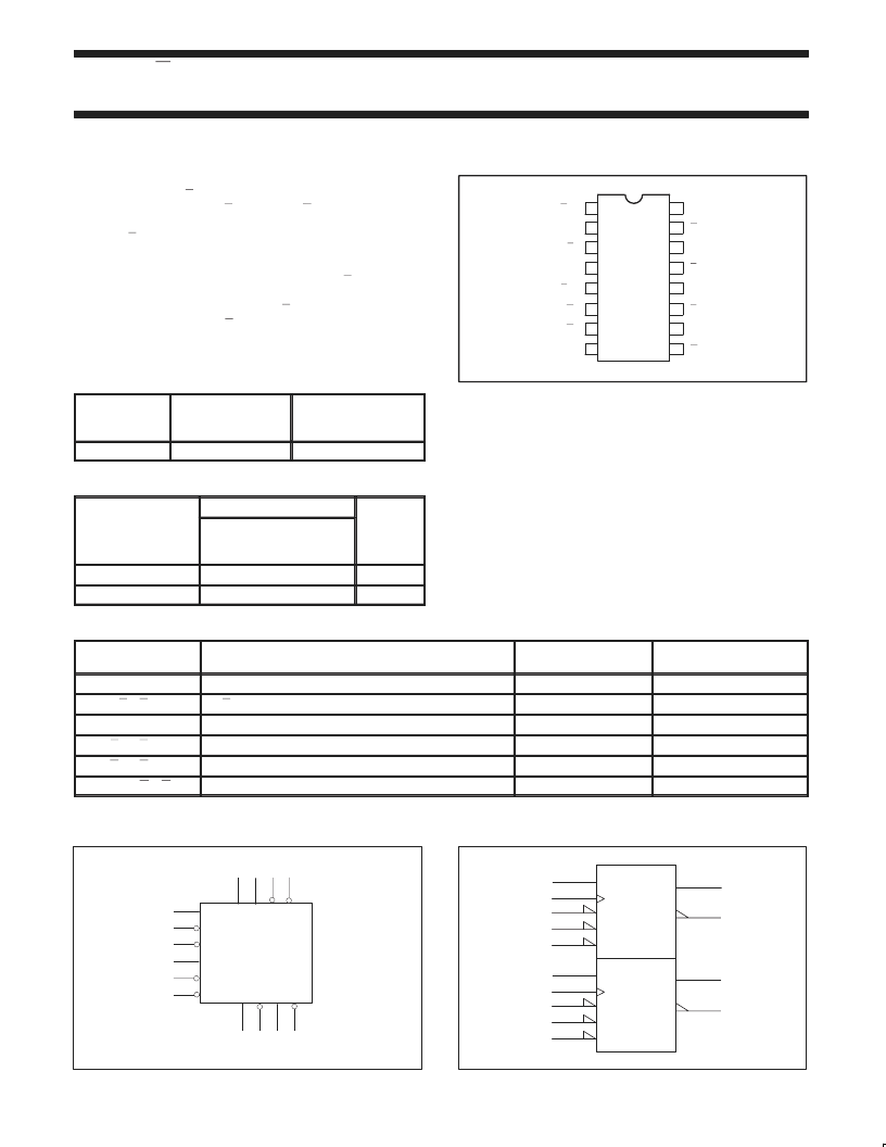
PIN CONFIGURATION
16
15
14
13
12
11
10
7
6
5
4
3
2
1
Q0
V
CC
CP1
SD1
Q1
K1
RD1
J1
RD0
J0
Q0
K0
CP0
SD0
9
8
GND
Q1
SF00135
INPUT AND OUTPUT LOADING AND FAN-OUT TABLE
PINS
DESCRIPTION
74ALS (U.L.)
HIGH/LOW
LOAD VALUE
HIGH/LOW
J0, J1
J inputs
1.0/2.0
20
μ
A/0.2mA
20
μ
A/0.2mA
20
μ
A/0.2mA
20
μ
A/0.4mA
20
μ
A/0.4mA
K0, K1
K inputs
1.0/2.0
CP0, CP1
Clock inputs (active rising edge)
1.0/2.0
SD0, SD1
Set inputs (active-Low)
1.0/4.0
RD0, RD1
Reset inputs (active-Low)
1.0/4.0
Q0, Q1, Q0, Q1
NOTE:
One (1.0) ALS unit load is defined as: 20
μ
A in the High state and 0.1mA in the Low state.
Data outputs
20/80
0.4mA/8mA
LOGIC SYMBOL
J1
J0
Q0 Q0 Q1 Q1
V
= Pin 16
GND = Pin 8
K1
K0
2 14 3 13
6 7 10 9
CP0
SD0
RD0
CP1
SD1
RD1
4
5
1
12
11
15
SF00136
IEC/IEEE SYMBOL
SF00137
7
2
4
3
1
5
14
12
13
15
11
6
10
9
1J
C1
1K
R
S
2J
C2
2K
R
S
相关PDF资料 |
PDF描述 |
|---|---|
| 74ALS109AD | Dual J-K positive edge-triggered flip-flop with set and reset |
| 74ALS109AN | Dual J-K positive edge-triggered flip-flop with set and reset |
| 74ALS10A | Triple 3-Input NAND gate |
| 74ALS10AD | Triple 3-Input NAND gate |
| 74ALS10AN | Triple 3-Input NAND gate |
相关代理商/技术参数 |
参数描述 |
|---|---|
| 74ALS109AD | 制造商:PHILIPS 制造商全称:NXP Semiconductors 功能描述:Dual J-K positive edge-triggered flip-flop with set and reset |
| 74ALS109AN | 制造商:PHILIPS 制造商全称:NXP Semiconductors 功能描述:Dual J-K positive edge-triggered flip-flop with set and reset |
| 74ALS109ANNSC91 | 制造商:National Semiconductor 功能描述:74ALS109N |
| 74ALS10A | 制造商:PHILIPS 制造商全称:NXP Semiconductors 功能描述:Triple 3-Input NAND gate |
| 74ALS10AD | 制造商:PHILIPS 制造商全称:NXP Semiconductors 功能描述:Triple 3-Input NAND gate |
发布紧急采购,3分钟左右您将得到回复。