- 您现在的位置:买卖IC网 > PDF目录360409 > 74ALS109A (NXP Semiconductors N.V.) Dual J-K positive edge-triggered flip-flop with set and reset PDF资料下载
参数资料
| 型号: | 74ALS109A |
| 厂商: | NXP Semiconductors N.V. |
| 英文描述: | Dual J-K positive edge-triggered flip-flop with set and reset |
| 中文描述: | 双JK上升沿触发器设置和复位触发器 |
| 文件页数: | 4/9页 |
| 文件大小: | 93K |
| 代理商: | 74ALS109A |
Philips Semiconductors
Product specification
74ALS109A
Dual J-K positive edge triggered flip-flop
with set and reset
1991 Feb 08
4
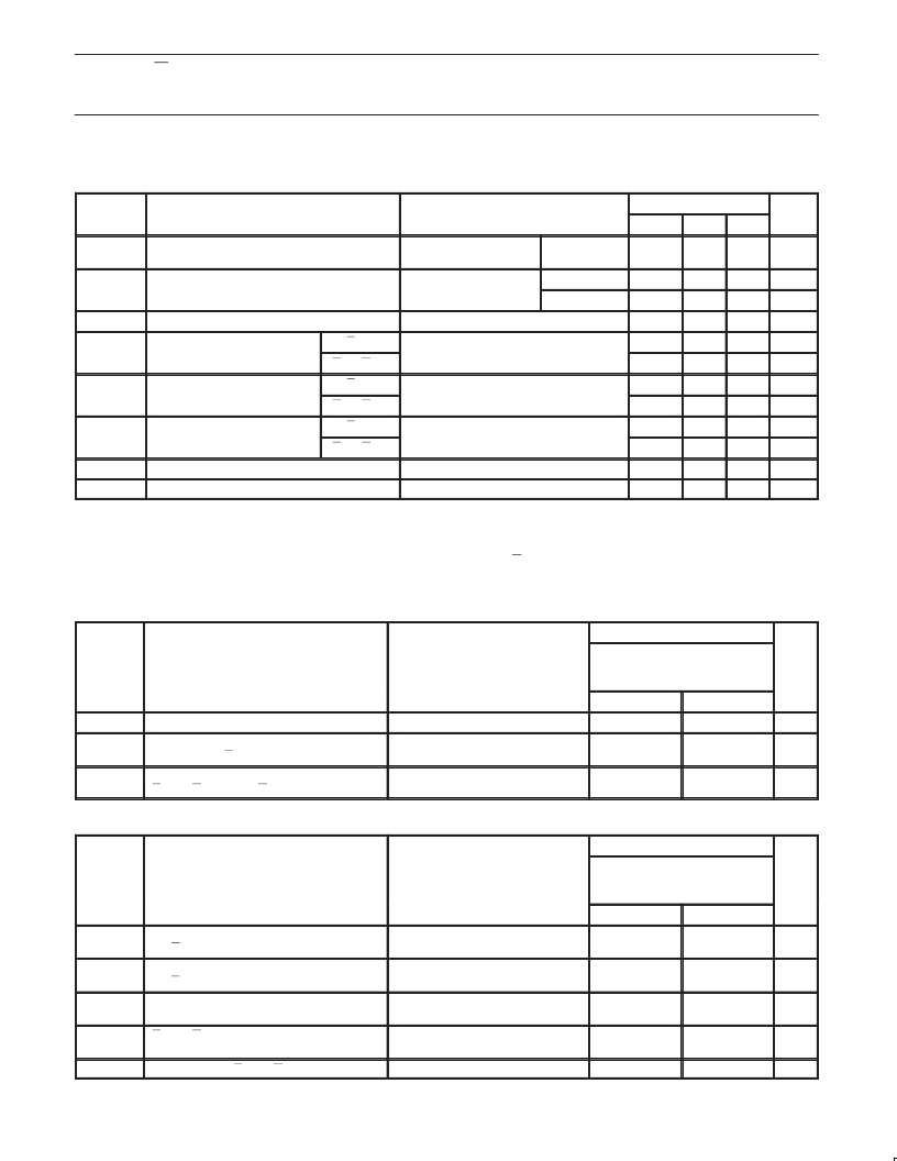
DC ELECTRICAL CHARACTERISTICS
(Over recommended operating free-air temperature range unless otherwise noted.)
SYMBOL
PARAMETER
TEST CONDITIONS
1
LIMITS
UNIT
MIN
TYP
2
MAX
V
OH
High-level output voltage
V
CC
=
±
10%,
V
IL
= MAX, V
IH
= MIN
I
OH
= –0.4mA
V
CC
– 2
V
V
OL
Low level output voltage
Low-level output voltage
V
= MIN, V
= MAX,
CC
V
IH
= MIN
I
OL
= 4mA
I
OL
= 8mA
0.25
0.40
V
IL
0.35
0.50
V
V
IK
Input clamp voltage
V
CC
= MIN, I
I
= I
IK
–0.73
–1.5
V
I
I
Input current at maximum input
voltage
Jn, Kn, CPn
V
CC
= MAX V = 7 0V
I
= 7.0V
0.1
mA
SDn, RDn
0.2
mA
I
IH
High level input current
High–level input current
Jn, Kn, CPn
V
CC
= MAX V = 2 7V
I
= 2.7V
20
μ
A
SDn, RDn
40
μ
A
I
IL
Low level input current
Low–level input current
Jn, Kn, CPn
V
CC
= MAX V = 0 4V
I
= 0.4V
–0.2
mA
SDn, RDn
–0.4
mA
I
O
I
CC
Output current
3
Supply current (total)
4
V
CC
= MAX, V
O
= 2.25V
V
CC
= MAX
–30
–112
mA
3.0
4.0
mA
NOTES:
1. For conditions shown as MIN or MAX, use the appropriate value specified under recommended operating conditions for the applicable type.
2. All typical values are at V
CC
= 5V, T
amb
= 25
°
C.
3. The output conditions have been chosen to produce a current that closely approximates one half of the true short–circuit output current, I
OS
.
4. Measure I
CC
with the clock input grounded and all outputs open, then with Q and Q outputs High in turn.
AC ELECTRICAL CHARACTERISTICS
LIMITS
SYMBOL
PARAMETER
TEST CONDITION
T
amb
= 0
°
C to +70
°
C
V
CC
= +5.0V
±
10%
C
L
= 50pF, R
L
= 500
UNIT
MIN
MAX
f
MAX
t
PLH
t
PHL
t
PLH
t
PHL
Maximum clock frequency
Waveform 1
80
MHz
Propagation delay
CPn to Qn or Qn
Waveform 1
3.0
3.0
14.0
14.0
ns
Propagation delay
SDn or RD to Qn or Qn
Waveform 2, 3
1.0
3.0
8.0
10.0
ns
AC SETUP REQUIREMENTS
LIMITS
SYMBOL
PARAMETER
TEST CONDITION
T
amb
= 0
°
C to +70
°
C
V
= +5.0V
±
10%
C
L
= 50pF, R
L
= 500
UNIT
MIN
MAX
t
su
(H)
t
su
(L)
t
h
(H
)
t
h
(
L
)
t
w
(H)
t
w
(L)
Setup time, High or Low
Jn, Kn to CPn
Waveform 1
6.0
6.0
ns
Hold time, High or Low
Jn, Kn to CPn
Waveform 1
0.0
0.0
ns
CPn Pulse width
High or Low
Waveform 1
6.0
6.0
ns
t
w
(L)
SDn or RDn Pulse width
Low
Waveform 2, 3
6.0
ns
t
rec
Recovery time, SDn or RDn to CPn
Waveform 2, 3
6.0
ns
相关PDF资料 |
PDF描述 |
|---|---|
| 74ALS109AD | Dual J-K positive edge-triggered flip-flop with set and reset |
| 74ALS109AN | Dual J-K positive edge-triggered flip-flop with set and reset |
| 74ALS10A | Triple 3-Input NAND gate |
| 74ALS10AD | Triple 3-Input NAND gate |
| 74ALS10AN | Triple 3-Input NAND gate |
相关代理商/技术参数 |
参数描述 |
|---|---|
| 74ALS109AD | 制造商:PHILIPS 制造商全称:NXP Semiconductors 功能描述:Dual J-K positive edge-triggered flip-flop with set and reset |
| 74ALS109AN | 制造商:PHILIPS 制造商全称:NXP Semiconductors 功能描述:Dual J-K positive edge-triggered flip-flop with set and reset |
| 74ALS109ANNSC91 | 制造商:National Semiconductor 功能描述:74ALS109N |
| 74ALS10A | 制造商:PHILIPS 制造商全称:NXP Semiconductors 功能描述:Triple 3-Input NAND gate |
| 74ALS10AD | 制造商:PHILIPS 制造商全称:NXP Semiconductors 功能描述:Triple 3-Input NAND gate |
发布紧急采购,3分钟左右您将得到回复。