- 您现在的位置:买卖IC网 > PDF目录360417 > 74ALVCH16543 (NXP Semiconductors N.V.) Quadruple Positive-NAND Gates With Schmitt-Trigger Inputs 14-SO -40 to 85 PDF资料下载
参数资料
| 型号: | 74ALVCH16543 |
| 厂商: | NXP Semiconductors N.V. |
| 英文描述: | Quadruple Positive-NAND Gates With Schmitt-Trigger Inputs 14-SO -40 to 85 |
| 中文描述: | 16位D登记收发器型;三态 |
| 文件页数: | 2/20页 |
| 文件大小: | 89K |
| 代理商: | 74ALVCH16543 |
1999 Nov 23
2
Philips Semiconductors
Product specification
16-bit D-type registered transceiver; 3-state
74ALVCH16543
FEATURES
In accordance with JEDEC standard no 8-1A
CMOS low power consumption
Direct interface with TTL levels
MULTIBYTE
flow-through pin-out architecture
16-bit transceiver with D-type latch
Combines 16245 and 16373 type functions in one chip
Back-to-back registers for storage
Output drive capability 50
transmission lines at 85
°
C
Separate controls for data flow in each direction
All data inputs have bus hold
3-state non-inverting outputs for bus oriented
applications
Current drive
±
24 mA at 3.0 V.
DESCRIPTION
The 74ALVCH16543 is a dual octal registered transceiver.
Each section contains two sets of D-type latches for
temporary storage of the data flow in either direction.
Separate latch enable (nLE
AB
, nLE
BA
) and output enable
(nOE
AB
, nOE
BA
) inputs are provided for each register to
permit independent control in either direction of the data
flow.
The ‘16543’ contains two sections each consisting of two
sets of eight D-type latches with separate inputs and
controls for each set. For data flow from A to B, for
example, the A-to-B enable (nE
AB
, where n equals 1 or 2)
inputsmustbeLOWinordertoenterdatafromnA
0
to nA
7
,
or take data from nB
0
to nB
7
, as indicated in the function
table. With nE
AB
LOW, a LOW signal on the A-to-B latch
enable (nLE
AB
) input makes the A-to-B latches
transparent; a subsequent LOW-to-HIGH transition of the
nLE
AB
signal stores the A data into the latches. With nE
AB
and nOE
AB
both LOW, the 3-state B output buffers are
active and display the data present at the output of the
A latches. Similarly, the nE
BA
, nLE
BA
and nOE
BA
signals
control the data flow from B-to-A.
Active bus hold circuitry is provided to hold unused or
floating data inputs at a valid logic level.
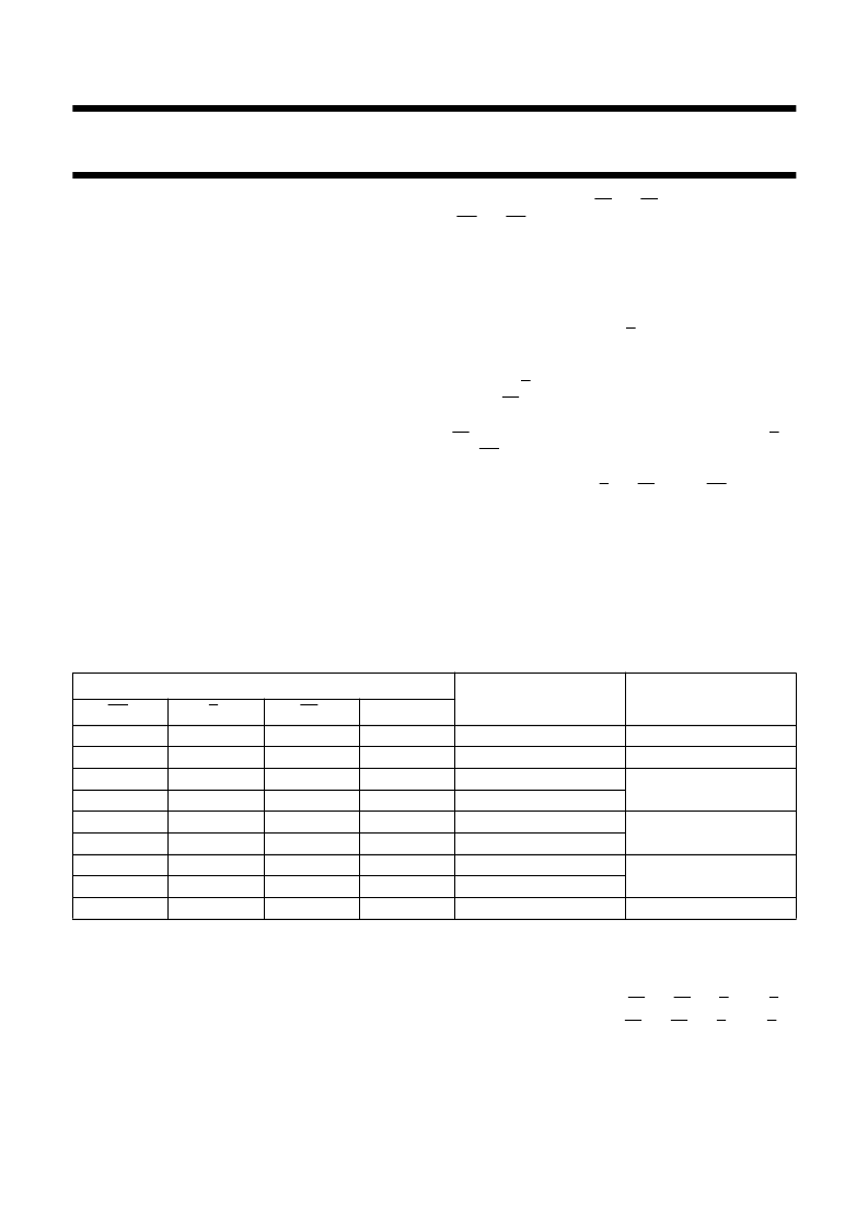
FUNCTION TABLE
See note 1.
Note
1.
XX = AB for A-to-B direction, BA for B-to-A direction;
H = HIGH voltage level; L = LOW voltage level;
h = HIGH state must be present one set-up time before the LOW-to-HIGH transition of nLE
AB
, nLE
BA
, nE
AB
or nE
BA
;
l = LOW state must be present one set-up time before the LOW-to-HIGH transition of nLE
AB
, nLE
BA
, nE
AB
or nE
BA
;
X = don’t care; NC = no change;
↑
= LOW-to-HIGH level transition;
Z = high-impedance OFF-state.
INPUTS
OUTPUTS
STATUS
nOE
XX
H
X
L
L
L
L
L
L
L
nE
XX
X
H
↑
↑
L
L
L
L
L
nLE
XX
X
X
L
L
↑
↑
L
L
H
nB
n
, nA
n
X
X
h
l
h
l
H
L
X
Z
Z
Z
Z
H
L
H
L
NC
disabled
disabled
disabled and latch
latch and display
transparent
hold
相关PDF资料 |
PDF描述 |
|---|---|
| 74ALVCH16600 | 18-bit universal bus transceiver 3-State |
| 74ALVCH16601 | Quadruple Positive-NAND Gates With Schmitt-Trigger Inputs 14-TSSOP -40 to 85 |
| 74ALVCH16623DGG | 16-bit transceiver with dual enable; 3-state |
| 74ALVCH16623 | 16-bit transceiver with dual enable; 3-state |
| 74ALVCH16646 | Quadruple Positive-NAND Gates With Schmitt-Trigger Inputs 14-TSSOP -40 to 85 |
相关代理商/技术参数 |
参数描述 |
|---|---|
| 74ALVCH16543DG | 功能描述:总线收发器 16-BIT LATCH XCVR 3-S RoHS:否 制造商:Fairchild Semiconductor 逻辑类型:CMOS 逻辑系列:74VCX 每芯片的通道数量:16 输入电平:CMOS 输出电平:CMOS 输出类型:3-State 高电平输出电流:- 24 mA 低电平输出电流:24 mA 传播延迟时间:6.2 ns 电源电压-最大:2.7 V, 3.6 V 电源电压-最小:1.65 V, 2.3 V 最大工作温度:+ 85 C 封装 / 箱体:TSSOP-48 封装:Reel |
| 74ALVCH16543DGG | 制造商:PHILIPS 制造商全称:NXP Semiconductors 功能描述:16-bit D-type registered transceiver; 3-state |
| 74ALVCH16543DGG,11 | 功能描述:总线收发器 16-BIT LATCH XCVR RoHS:否 制造商:Fairchild Semiconductor 逻辑类型:CMOS 逻辑系列:74VCX 每芯片的通道数量:16 输入电平:CMOS 输出电平:CMOS 输出类型:3-State 高电平输出电流:- 24 mA 低电平输出电流:24 mA 传播延迟时间:6.2 ns 电源电压-最大:2.7 V, 3.6 V 电源电压-最小:1.65 V, 2.3 V 最大工作温度:+ 85 C 封装 / 箱体:TSSOP-48 封装:Reel |
| 74ALVCH16543DGG,112 | 制造商:NXP Semiconductors 功能描述: |
| 74ALVCH16543DGG,118 | 制造商:NXP Semiconductors 功能描述: |
发布紧急采购,3分钟左右您将得到回复。