- 您现在的位置:买卖IC网 > PDF目录360417 > 74ALVCH16601 (NXP Semiconductors N.V.) Quadruple Positive-NAND Gates With Schmitt-Trigger Inputs 14-TSSOP -40 to 85 PDF资料下载
参数资料
| 型号: | 74ALVCH16601 |
| 厂商: | NXP Semiconductors N.V. |
| 英文描述: | Quadruple Positive-NAND Gates With Schmitt-Trigger Inputs 14-TSSOP -40 to 85 |
| 中文描述: | 18位通用总线收发器,三态 |
| 文件页数: | 10/12页 |
| 文件大小: | 86K |
| 代理商: | 74ALVCH16601 |
Philips Semiconductors
Product specification
74ALVCH16601
18-bit universal bus transceiver (3-State)
1998 Sep 24
10
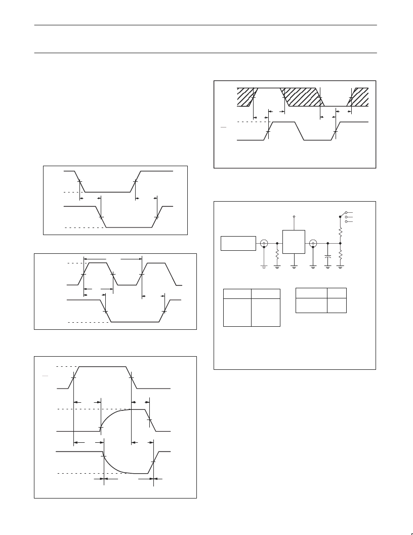
AC WAVEFORMS
V
= 2.3 TO 2.7 V RANGE
1. V
M
= 0.5 V
2. V
X
= V
OL
+ 0.15V
3. V
Y
= V
OH
– 0.15V
4. V
I
= V
CC
5. V
OL
and V
OH
are the typical output voltage drop that occur with
the output load.
V
CC
= 3.0 TO 3.6 V RANGE AND V
CC
= 2.7 V
1. V
M
= 1.5 V
2. V
X
= V
OL
+ 0.3V
3. V
Y
= V
OH
– 0.3V
4. V
I
= 2.7 V
5. V
OL
and V
OH
are the typical output voltage drop that occur with
the output load.
SW00063
An, Bn
INPUT
V
M
t
PHL
t
PLH
V
OL
V
I
V
M
GND
V
OH
Bn, An
OUTPUT
Waveform 1. Input (An, Bn) to output (Bn, An) propagation
delays
SW00134
CP
INPUT
V
M
t
PHL
t
PLH
V
OL
V
I
V
M
GND
V
OH
An, Bn
OUTPUT
t
W
LE
INPUT
1/f
max
Waveform 2. Latch enable input (LE
AB
, LE
BA
) and clock pulse
input (CP
AB
, CP
BA
) to output propagation delays and their
pulse width
t
PLZ
t
PZL
V
I
OE
XX
INPUT
GND
V
CC
OUTPUT
LOW-to-OFF
OFF-to-LOW
V
OL
V
OH
OUTPUT
HIGH-to-OFF
OFF-to-HIGH
GND
outputs
en-
abled
outputs
en-
abled
outputs
dis-
abled
t
PHZ
V
M
V
M
V
M
t
PZH
V
X
V
Y
SW00127
Waveform 3. 3-State enable and disable times
éééééééé
éééééééé
éééééééé
V
M
An, Bn
INPUT
V
M
t
SU
NOTE:
The unshaded areas indicate when the input is permitted
to change for predictable output performance.
SW00128
t
SU
t
h
V
I
GND
V
I
GND
CP
, LE
XX
INPUT
Waveform 4. Data set-up and hold times for the An and Bn
inputs to the LE
AB
, LE
BA
, CP
AB
and CP
BA
inputs
TEST CIRCUIT
PULSE
GENERATOR
R
T
V
IN
D.U.T.
V
OUT
C
L
V
CC
R
L
=500
SWITCH POSITION
TEST
t
PLH
/t
PHL
t
PLZ
/t
PZL
t
PHZ
/t
PZH
SWITCH
Open
2
V
CC
GND
Test Circuit for 3-State Outputs
Open
GND
S
1
2
V
CC
DEFINITIONS
R
L
= Load resistor
C
L
= Load capacitance includes jig and probe capacitance
R
T
=Termination resistance should be equal to Z
OUT
of pulse generators.
V
CC
2.7V
2.7 – 3.6V
V
IN
V
CC
2.7V
SW00047
R
L
=500
Load circuitry for switching times
相关PDF资料 |
PDF描述 |
|---|---|
| 74ALVCH16623DGG | 16-bit transceiver with dual enable; 3-state |
| 74ALVCH16623 | 16-bit transceiver with dual enable; 3-state |
| 74ALVCH16646 | Quadruple Positive-NAND Gates With Schmitt-Trigger Inputs 14-TSSOP -40 to 85 |
| 74ALVCH16652 | 16-bit transceiver/register with dual enable; 3-state |
| 74ALVCH16821 | Quadruple Positive-NAND Gates With Schmitt-Trigger Inputs 14-TSSOP -40 to 85 |
相关代理商/技术参数 |
参数描述 |
|---|---|
| 74ALVCH16601DG | 功能描述:总线收发器 18-BIT UNIV BUS XCVR 3-STATE RoHS:否 制造商:Fairchild Semiconductor 逻辑类型:CMOS 逻辑系列:74VCX 每芯片的通道数量:16 输入电平:CMOS 输出电平:CMOS 输出类型:3-State 高电平输出电流:- 24 mA 低电平输出电流:24 mA 传播延迟时间:6.2 ns 电源电压-最大:2.7 V, 3.6 V 电源电压-最小:1.65 V, 2.3 V 最大工作温度:+ 85 C 封装 / 箱体:TSSOP-48 封装:Reel |
| 74ALVCH16601DGG | 制造商:PHILIPS 制造商全称:NXP Semiconductors 功能描述:18-bit universal bus transceiver 3-State |
| 74ALVCH16601DGG,11 | 功能描述:总线收发器 18-BIT UNIV BUS RoHS:否 制造商:Fairchild Semiconductor 逻辑类型:CMOS 逻辑系列:74VCX 每芯片的通道数量:16 输入电平:CMOS 输出电平:CMOS 输出类型:3-State 高电平输出电流:- 24 mA 低电平输出电流:24 mA 传播延迟时间:6.2 ns 电源电压-最大:2.7 V, 3.6 V 电源电压-最小:1.65 V, 2.3 V 最大工作温度:+ 85 C 封装 / 箱体:TSSOP-48 封装:Reel |
| 74ALVCH16601DGG,112 | 制造商:NXP Semiconductors 功能描述: |
| 74ALVCH16601DGG,118 | 制造商:NXP Semiconductors 功能描述: |
发布紧急采购,3分钟左右您将得到回复。