参数资料
| 型号: | 74LVC1G00FW4-7 |
| 厂商: | Diodes Inc |
| 文件页数: | 1/15页 |
| 文件大小: | 0K |
| 描述: | IC GATE NAND SGL 2INP DFN1010-6 |
| 标准包装: | 1 |
| 系列: | 74LVC |
| 逻辑类型: | 与非门 |
| 电路数: | 1 |
| 输入数: | 2 |
| 电源电压: | 1.65 V ~ 5.5 V |
| 电流 - 静态(最大值): | 200µA |
| 输出电流高,低: | 32mA,32mA |
| 逻辑电平 - 低: | 0.7 V ~ 0.8 V |
| 逻辑电平 - 高: | 1.7 V ~ 2 V |
| 额定电压和最大 CL 时的最大传播延迟: | 1.8ns @ 5V,50pF |
| 工作温度: | -40°C ~ 125°C |
| 安装类型: | 表面贴装 |
| 供应商设备封装: | DFN1010 |
| 封装/外壳: | 6-XFDFN |
| 包装: | 标准包装 |
| 其它名称: | 74LVC1G00FW4-7DIDKR |
74LVC1G00
Document number: DS32196 Rev. 7 - 2
1 of 15
www.diodes.com
March 2014
Diodes Incorporated
NEW
PROD
UC
T
74LVC1G00
SINGLE 2 INPUT POSITIVE NAND GATE
Description
The 74LVC1G00 is a single 2-input positive NAND gate with a
standard push-pull output. The device is designed for operation with
a power supply range of 1.65V to 5.5V. The inputs are tolerant to
5.5V allowing this device to be used in a mixed voltage environment.
The device is fully specified for partial power down applications using
IOFF. The IOFF circuitry disables the output preventing damaging
current backflow when the device is powered down.
The gate performs the positive Boolean function:
B
A
Y
=
or
B
A
Y
+
=
Features
Wide Supply Voltage Range from 1.65 to 5.5V
± 24mA Output Drive at 3.3V
CMOS low power consumption
IOFF Supports Partial-Power-Down Mode Operation
Inputs accept up to 5.5V
ESD Protection Tested per JESD 22
o
Exceeds 200-V Machine Model (A115)
o
Exceeds 2000-V Human Body Model (A114)
o
Exceeds 1000-V Charged Device Model (C101)
Latch-Up Exceeds 100mA per JESD 78, Class I
Range of Package Options
Direct Interface with TTL Levels
Totally Lead-Free & Fully RoHS Compliant (Notes 1 & 2)
Halogen and Antimony Free. “Green” Device (Note 3)
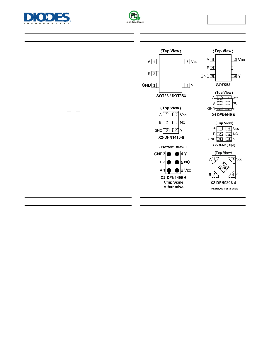
Pin Assignments
Applications
Voltage Level Shifting
General Purpose Logic
Power Down Signal Isolation
Wide array of products such as.
o
PCs, networking, notebooks, netbooks, PDAs
o
Tablet Computers, E-readers
o
Computer peripherals, hard drives, CD/DVD ROM
o
TV, DVD, DVR, set top box
o
Cell Phones, Personal Navigation / GPS
o
MP3 players ,Cameras, Video Recorders
Notes:
1. No purposely added lead. Fully EU Directive 2002/95/EC (RoHS) & 2011/65/EU (RoHS 2) compliant.
2. See http://www.diodes.com for more information about Diodes Incorporated’s definitions of Halogen- and Antimony-free, "Green" and Lead-free.
3. Halogen- and Antimony-free "Green” products are defined as those which contain <900ppm bromine, <900ppm chlorine (<1500ppm total Br + Cl)
and < 1000 ppm antimony compounds.
Future
Product
相关PDF资料 |
PDF描述 |
|---|---|
| 74LVC1G00GW,165 | IC SNGL 2-IN NAND GATE 5TSSOP |
| 74LVC1G02GW,165 | IC SNGL 2-IN NOR GATE 5TSSOP |
| 74LVC1G02Z-7 | IC GATE NOR SGL 2INP SOT553 |
| 74LVC1G04Z-7 | IC GATE INVERTER SNGL 1IN SOT553 |
| 74LVC1G06Z-7 | IC SGL INV GATE OD SOT553 |
相关代理商/技术参数 |
参数描述 |
|---|---|
| 74LVC1G00FW5-7 | 功能描述:NAND Gate IC 1 Channel X1-DFN1010-6 制造商:diodes incorporated 系列:74LVC 包装:剪切带(CT) 零件状态:有效 逻辑类型:与非门 电路数:1 输入数:2 特性:- 电压 - 电源:1.65 V ~ 5.5 V 电流 - 静态(最大值):200μA 电流 - 输出高,低:32mA,32mA 逻辑电平 - 低:0.7 V ~ 0.8 V 逻辑电平 - 高:1.7 V ~ 2 V 不同 V,最大 CL 时的最大传播延迟:5.5ns @ 5V,50pF 工作温度:-40°C ~ 125°C 安装类型:表面贴装 供应商器件封装:X1-DFN1010-6 封装/外壳:6-XDFN 标准包装:1 |
| 74LVC1G00FX4-7 | 功能描述:NAND Gate IC 1 Channel X2-DFN1409-6 制造商:diodes incorporated 系列:74LVC 包装:剪切带(CT) 零件状态:有效 逻辑类型:与非门 电路数:1 输入数:2 特性:- 电压 - 电源:1.65 V ~ 5.5 V 电流 - 静态(最大值):200μA 电流 - 输出高,低:32mA,32mA 逻辑电平 - 低:0.7 V ~ 0.8 V 逻辑电平 - 高:1.7 V ~ 2 V 不同 V,最大 CL 时的最大传播延迟:5.5ns @ 5V,50pF 工作温度:-40°C ~ 125°C 安装类型:表面贴装 供应商器件封装:X2-DFN1409-6 封装/外壳:6-XFDFN 标准包装:1 |
| 74LVC1G00FZ4-7 | 功能描述:逻辑门 1.65 to 5.5V VCC 1G Single 2-Input NAND RoHS:否 制造商:Texas Instruments 产品:OR 逻辑系列:LVC 栅极数量:2 线路数量(输入/输出):2 / 1 高电平输出电流:- 16 mA 低电平输出电流:16 mA 传播延迟时间:3.8 ns 电源电压-最大:5.5 V 电源电压-最小:1.65 V 最大工作温度:+ 125 C 安装风格:SMD/SMT 封装 / 箱体:DCU-8 封装:Reel |
| 74LVC1G00GF | 制造商:NXP Semiconductors 功能描述:IC 2 INPUT NAND-GATE XSON6 制造商:NXP Semiconductors 功能描述:IC, 2 INPUT NAND-GATE, XSON6, Logic Type:NAND Gate, Output Current:32mA, No. of |
| 74LVC1G00GF,132 | 功能描述:逻辑门 3.3V SINGLE 2-INPUT RoHS:否 制造商:Texas Instruments 产品:OR 逻辑系列:LVC 栅极数量:2 线路数量(输入/输出):2 / 1 高电平输出电流:- 16 mA 低电平输出电流:16 mA 传播延迟时间:3.8 ns 电源电压-最大:5.5 V 电源电压-最小:1.65 V 最大工作温度:+ 125 C 安装风格:SMD/SMT 封装 / 箱体:DCU-8 封装:Reel |
发布紧急采购,3分钟左右您将得到回复。