- 您现在的位置:买卖IC网 > PDF目录162995 > 844S012BKI-01LF (INTEGRATED DEVICE TECHNOLOGY INC) OTHER CLOCK GENERATOR, QCC56 PDF资料下载
参数资料
| 型号: | 844S012BKI-01LF |
| 厂商: | INTEGRATED DEVICE TECHNOLOGY INC |
| 元件分类: | 时钟产生/分配 |
| 英文描述: | OTHER CLOCK GENERATOR, QCC56 |
| 封装: | 8 X 8 MM, 0.925 MM HEIGHT, ROHS COMPLIANT, MO-220VLLD-2, VFQFN-56 |
| 文件页数: | 17/23页 |
| 文件大小: | 847K |
| 代理商: | 844S012BKI-01LF |
ICS844S012BKI-01 REVISION A APRIL 2, 2010
3
2010 Integrated Device Technology, Inc.
ICS844S012I-01 Data Sheet
CRYSTAL-TO-LVDS/LVCMOS FREQUENCY SYNTHESIZER
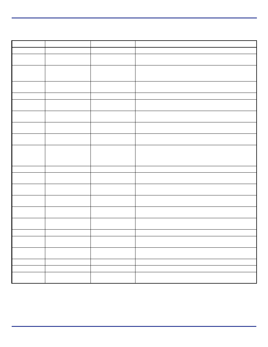
Table 1. Pin Descriptions
NOTE: Pullup and Pulldown refer to internal input resistors. See Table 2, Pin Characteristics, for typical values.
Number
Name
Type
Description
1VDDO_REF
Power
Output supply pin for REF_OUT outputs.
2,
3
REF_OUT0,
REF_OUT1
Output
Single-ended reference clock outputs. 23
typical output
impedance. LVCMOS/LVTTL interface levels.
4, 5, 15,
27, 34, 35, 36,
40, 46, 50, 54
GND
Power
Power supply ground.
6
REF_IN
Input
Pulldown
Single-ended reference clock input. LVCMOS/LVTTL interface
levels.
7, 14, 28, 29
VDD
Power
Core supply pins.
8
REF_SEL
Input
Pulldown
Reference select pin. When HIGH selects REF_IN. When LOW,
selects crystal. See Table 3E. LVCMOS/LVTTL interface levels.
9,
10
XTAL_IN
XTAL_OUT
Input
Crystal oscillator interface. XTAL_IN is the input, XTAL_OUT is the
output.
11
BYPASS
Input
Pulldown
PLL bypass. When HIGH, bypasses PLL. When LOW, selects PLL.
See Table 3J. LVCMOS/LVTTL interface levels..
12
REF_OE
Input
Pulldown
Active HIGH REF_OUT enable/disable pin. See Table 3F.
LVCMOS/LVTTL interface levels.
13
nMR
Input
Pullup
Active LOW Master Reset. When logic LOW, the internal dividers
are reset. When logic HIGH, the internal dividers are enabled. This
device requires a reset signal after powerup. See Table 3G.
LVCMOS/LVTTL interface levels.
16, 17
SSC1, SSC0
Input
Pullup
SSC control pins. See Table 3D. LVCMOS/LVTTL interface levels.
18,
19, 20
F_SELB2,
F_SELB1, F_SELB0
Input
Pulldown
Frequency select pins for QBx outputs. See Table 3B.
LVCMOS/LVTTL interface levels.
21,
22, 23
F_SELC2,
F_SELC1, F_SELC0
Input
Pulldown
Frequency select pins for QC output. See Table 3C.
LVCMOS/LVTTL interface levels.
24, 25
F_SELA1, F_SELA0
Input
Pulldown
Frequency select pins for QAx, nQAx outputs. See Table 3A.
LVCMOS/LVTTL interface levels.
26
QA_OE
Input
Pullup
Output enable pin for Bank A outputs. See Table 3H.
LVCMOS/LVTTL interface levels.
30, 31
32, 33
nQA1, QA1
nQA0, QA0
Output
Differential Bank A clock output pairs. LVDS interface levels.
37, 38
VDDA
Power
Analog supply pins.
39
QBC_OE
Input
Pullup
Output enable pin for Bank B and Bank C outputs. See Table 3I.
LVCMOS/LVTTL Interface levels.
41
QC
Output
Single-ended Bank C clock output. LVCMOS/LVTTL interface
levels. 18
typical output impedance.
42
VDDOC
Power
Output supply pin for QC LVCMOS output.
43, 48, 52, 56
VDDOB
Power
Output supply pins for QBx LVCMOS outputs.
44, 45, 47,
49, 51, 53, 55
QB0, QB1, QB2,
QB3, QB4, QB5, QB6
Output
Single-ended Bank B clock outputs. LVCMOS/LVTTL interface
levels. 18
typical output impedance.
相关PDF资料 |
PDF描述 |
|---|---|
| 845730021 | INTERCONNECTION DEVICE |
| 845730023 | INTERCONNECTION DEVICE |
| 845730024 | INTERCONNECTION DEVICE |
| 845979013 | INTERCONNECTION DEVICE |
| 845979019 | INTERCONNECTION DEVICE |
相关代理商/技术参数 |
参数描述 |
|---|---|
| 844S0258BK-07LF | 制造商:Integrated Device Technology Inc 功能描述:32 VFQFN (LEAD-FREE) - Bulk |
| 844S0258BK-07LFT | 制造商:Integrated Device Technology Inc 功能描述:32 VFQFN (LEAD-FREE) - Tape and Reel |
| 844S0258CK-07LF | 制造商:IDT from Components Direct 功能描述:IDT 844S0258CK-07LF CLOCKS - TIMERS - Trays 制造商:IDT 功能描述:IDT 844S0258CK-07LF Clocks - Timers |
| 844S2416AKI | 制造商:Integrated Device Technology Inc 功能描述:CLK GEN VFQFN56 - Bulk |
| 844S2416BKI | 制造商:Integrated Device Technology Inc 功能描述:CLK GEN VFQFN56 - Bulk |
发布紧急采购,3分钟左右您将得到回复。