- 您现在的位置:买卖IC网 > PDF目录9511 > 8N3Q001EG-203LCDI8 (IDT, Integrated Device Technology Inc)IC CLCK OSC QUAD FREQUENCY 5X7 PDF资料下载
参数资料
| 型号: | 8N3Q001EG-203LCDI8 |
| 厂商: | IDT, Integrated Device Technology Inc |
| 文件页数: | 5/21页 |
| 文件大小: | 0K |
| 描述: | IC CLCK OSC QUAD FREQUENCY 5X7 |
| 特色产品: | Fourth-generation FemtoClock for VCXO |
| 标准包装: | 1 |
| 系列: | FemtoClock® NG |
| 类型: | 时钟振荡器 |
| 频率: | 可调节/可选择 |
| 电源电压: | 2.375 V ~ 3.465 V |
| 电流 - 电源: | 150mA |
| 工作温度: | -40°C ~ 85°C |
| 封装/外壳: | 10-CLCC |
| 包装: | 标准包装 |
| 供应商设备封装: | 10-CLCC |
| 安装类型: | 表面贴装 |
| 其它名称: | 800-2570-6 |
IDT8N3Q001 REV G Data Sheet
QUAD-FREQUENCY PROGRAMMABLE-XO
IDT8N3Q001GCD REVISION A MARCH 6, 2012
13
2012 Integrated Device Technology, Inc.
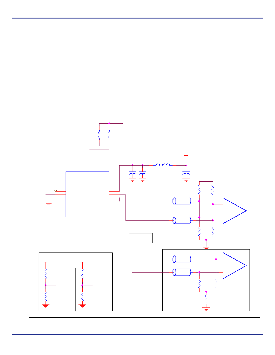
Schematic Layout
Figure 3 shows an example of IDT8N3Q001 application schematic.
In this example, the device is operated at VCC = 3.3V. As with any
high speed analog circuitry, the power supply pins are vulnerable to
noise. To achieve optimum jitter performance, power supply isolation
is required. The IDT8N3Q001 provides separate power supplies to
isolate from coupling into the internal PLL.
In order to achieve the best possible filtering, it is recommended that
the placement of the filter components be on the device side of the
PCB as close to the power pins as possible. If space is limited, the
0.1uF capacitor in each power pin filter should be placed on the
device side of the PCB and the other components can be placed on
the opposite side.
Power supply filter recommendations are a general guideline to be
used for reducing external noise from coupling into the devices. The
filter performance is designed for wide range of noise frequencies.
This low-pass filter starts to attenuate noise at approximately 10kHz.
If a specific frequency noise component is known, such as switching
power supply frequencies, it is recommended that component values
be adjusted and if required, additional filtering be added. Additionally,
good general design practices for power plane voltage stability
suggests adding bulk capacitances in the local area of all devices.
The schematic example focuses on functional connections and is not
configuration specific. Refer to the pin description and functional
tables in the datasheet to ensure the logic control inputs are properly
set.
Figure 3. IDT8N3Q001 Application Schematic
Zo = 50 Ohm
nQ
R7
50
RU2
Not Install
SC
LK
R3
133
SD
AT
A
Logic Control Input Examples
FS
E
L
1
R1
SP
VCC
+
-
BLM18BB221SN1
Ferrite Bead
1
2
RU1
1K
RD1
Not Install
Q
VCC
3.3V
R2
SP
R6
82.5
C3
0.1uF
VCC
OE
3.3V
To Logic
Input
pins
Set Logic
Input to
'0'
FS
E
L
0
R4
133
VCC
Zo = 50 Ohm
R9
50
R5
82.5
C1
0.1uF
Optional
Y-Termination
R8
50
To Logic
Input
pins
C2
10uF
Set Logic
Input to
'1'
Zo = 50 Ohm
U1
1
2
3
6
7
8
4
5
9
10
DNU
OE
VEE
Q
nQ
VCC
FS
E
L
0
FS
E
L
1
S
D
A
T
A
SC
LK
VCC=3.3V
+
-
RD2
1K
Zo = 50 Ohm
相关PDF资料 |
PDF描述 |
|---|---|
| MS27473E24B19SA | CONN PLUG 19POS STRAIGHT W/SCKT |
| V110A5M300B3 | CONVERTER MOD DC/DC 5V 300W |
| 8N3Q001EG-102LCDI8 | IC CLCK OSC QUAD FREQUENCY 5X7 |
| V110A5M300B | CONVERTER MOD DC/DC 5V 300W |
| V110A8M300BL2 | CONVERTER MOD DC/DC 8V 300W |
相关代理商/技术参数 |
参数描述 |
|---|---|
| 8N3Q001EG-204LCDI | 功能描述:时钟发生器及支持产品 RoHS:否 制造商:Silicon Labs 类型:Clock Generators 最大输入频率:14.318 MHz 最大输出频率:166 MHz 输出端数量:16 占空比 - 最大:55 % 工作电源电压:3.3 V 工作电源电流:1 mA 最大工作温度:+ 85 C 安装风格:SMD/SMT 封装 / 箱体:QFN-56 |
| 8N3Q001EG-204LCDI8 | 功能描述:IC CLCK OSC QUAD FREQUENCY 5X7 RoHS:是 类别:集成电路 (IC) >> 时钟/计时 - 可编程计时器和振荡器 系列:FemtoClock® NG 标准包装:3,000 系列:- 类型:振荡器 - 晶体 计数:- 频率:- 电源电压:2.3 V ~ 5.5 V 电流 - 电源:1.07mA 工作温度:-30°C ~ 80°C 封装/外壳:SOT-665 包装:带卷 (TR) 供应商设备封装:SS迷你型-5D 安装类型:表面贴装 其它名称:AN8955SSMTXLTR |
| 8N3Q001EG-2148CDI | 制造商:Integrated Device Technology Inc 功能描述:10-LEAD CERAMIC 5X7 - Bulk |
| 8N3Q001EG-2148CDI8 | 功能描述:Clock Oscillator IC 231.25MHz 10-CLCC 制造商:idt, integrated device technology inc 系列:FemtoClock? NG 包装:带卷(TR) 零件状态:有效 类型:时钟振荡器 计数:- 频率:231.25MHz 电压 - 电源:3.135 V ~ 3.465 V 电流 - 电源:140mA 工作温度:-40°C ~ 85°C 封装/外壳:10-CLCC 供应商器件封装:10-CLCC(7x5) 安装类型:表面贴装 标准包装:1,000 |
| 8N3Q001EG-2163CDI | 制造商:Integrated Device Technology Inc 功能描述:SMD Crystal Oscillator 3.3V 10-Pin CLCC Tray 制造商:Integrated Device Technology Inc 功能描述:10-LEAD CERAMIC 5X7 - Bulk |
发布紧急采购,3分钟左右您将得到回复。