- 您现在的位置:买卖IC网 > PDF目录24617 > 9161A-01CW16WLF (INTEGRATED DEVICE TECHNOLOGY INC) 120 MHz, VIDEO CLOCK GENERATOR, PDSO16 PDF资料下载
参数资料
| 型号: | 9161A-01CW16WLF |
| 厂商: | INTEGRATED DEVICE TECHNOLOGY INC |
| 元件分类: | 时钟产生/分配 |
| 英文描述: | 120 MHz, VIDEO CLOCK GENERATOR, PDSO16 |
| 封装: | 0.300 INCH, SOIC-16 |
| 文件页数: | 11/15页 |
| 文件大小: | 539K |
| 代理商: | 9161A-01CW16WLF |
5
ICS9161A
Serial Programming Architecture
The pins SEL0 and SEL1 perform the dual functions of select-
ing registers and serial programming. In serial programming
mode, SEL0 acts as a clock pin while SEL1 acts as the data pin.
The ICS9161A-01 may not be serially programmed when in
power-down mode.
In order to program a particular register, an unlocking sequence
must occur. The unlocking sequence is detailed in the following
timing diagram:
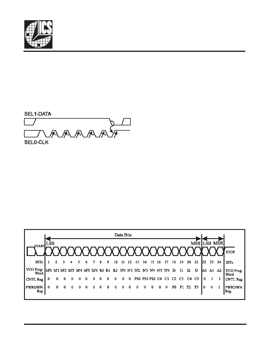
Serial Data Register
The serial data is clocked into the serial data register in the
order described in Figure 1 below (Serial Data Timing).
The serial data is sent as follows: An individual data bit is
sampled on the rising edge of CLK. The complement of the
data bit must be sampled on the previous falling edge of CLK.
The setup and hold time requirements must be met on both
CLK edges. For specifics on timing, see the timing diagrams
on pages 10, 11 and 12.
The bits are shifted in this order: a start bit, 21 data bits, 3
address bits (which designate the desired register), and a stop
bit. A total of 24 bits must always be loaded into the serial data
register or an error is issued. Following the entry of the last
data bit, a stop bit or load command is issued by bringing
DATA high and toggling CLK high-to-low and low-to-high.
The unlocking mechanism then resets itself following the
load. Only after a time-out period are the SEL0 and SEL1 pins
allowed to return to a register selection function.
Since the VCLK registers are selected by the SEL0 and SEL1
pins, and since any change in their state may affect the output
frequency, new data input on the selection bits is only permitted
to pass through the decode logic after the watchdog timer has
timed out. This delay of SEL0 or SEL1 data permits a serial
program cycle to occur without affecting the current register
selection.
The unlock sequence consists of at least five low-to-high
transitions of CLK while data is high, followed immediately
by a single low-to-high transition while data is low. Following
this unlock sequence, data can be loaded into the serial data
register. This programming must include the start bit, shown
in Figure 1.
Following any transition of CLK or DATA, the watchdog
timer is reset and begins counting. The watchdog timer
ensures that successive rising edges of CLK and DATA do not
violate the time-out specification of 2ms. If a time-out
occurs, the lock mechanism is reset and the data in the serial
data register is ignored.
Figure 1: Serial Data Timing
相关PDF资料 |
PDF描述 |
|---|---|
| 9161A-01CW16W | 120 MHz, VIDEO CLOCK GENERATOR, PDSO16 |
| 9162C | 2M X 32 FAST PAGE DRAM MODULE, 60 ns, SMA72 |
| 9163901MFA | QUAD LINE DRIVER, CDFP16 |
| 9163901MEA | QUAD LINE DRIVER, CDIP16 |
| 9163901M2A | QUAD LINE DRIVER, CQCC20 |
相关代理商/技术参数 |
参数描述 |
|---|---|
| 9-161A-R | 制造商:Cinch Connectors 功能描述: |
| 9161-CHR-BULK | 制造商:Belden Inc 功能描述: |
| 9-161-L | 制造商:Cinch Connectors 功能描述: |
| 9-161-R | 制造商:Cinch Connectors 功能描述:Conn Terminal Strip 9 POS 11.13mm Crimp ST Cable Mount |
| 9162 | 功能描述:PROTO-BOARD 14/16PIN SOIC SMD RoHS:是 类别:原型开发产品 >> 适配器,可互换接口板 系列:9000, Surfboards® 标准包装:1 系列:- 原型板类型:- Package Accepted:- 尺寸/尺寸:- 位置数:- 孔直径:- 板厚度:- 材质:- |
发布紧急采购,3分钟左右您将得到回复。