- 您现在的位置:买卖IC网 > PDF目录24623 > 9248BF-81LFT (INTEGRATED DEVICE TECHNOLOGY INC) 133.3 MHz, PROC SPECIFIC CLOCK GENERATOR, PDSO48 PDF资料下载
参数资料
| 型号: | 9248BF-81LFT |
| 厂商: | INTEGRATED DEVICE TECHNOLOGY INC |
| 元件分类: | 时钟产生/分配 |
| 英文描述: | 133.3 MHz, PROC SPECIFIC CLOCK GENERATOR, PDSO48 |
| 封装: | 0.300 INCH, GREEN, SSOP-48 |
| 文件页数: | 12/20页 |
| 文件大小: | 568K |
| 代理商: | 9248BF-81LFT |
2
ICS9248 -81I
Advance Information
0851—08/06/03
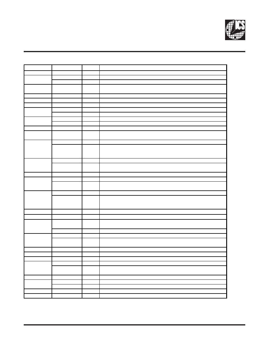
Pin Descriptions
Notes:
1:
Internal Pull-up Resistor of 120K to 3.3V on indicated inputs
2:
Bidirectional input/output pins, input logic levels are latched at internal power-on-reset. Use
10Kohm resistor to program logic Hi to VDD or GND for logic low.
Pin number
Pin name
Type
Description
1
VDDR/X
Power
Isolated 3.3 V power for crystal & reference
REF0
Output
3.3V, 14.318 MHz reference clock output.
Mode
Input
Function select pin, 1=desk top mode, 0=mobile mode. Latched input.
3,9,16,22,
27,33,39
GND
Power
3.3 V Ground
4
X1
Input
14.318 MHz crystal input
5
X2
Output
14.318 MHz crystal output
6,14
VDDPCI
Power
3.3 V power for the PCI clock outputs
FS1
Input
Logic input frequency select bit. Input latched at power-on.
PCICLK_F
Output
3.3 V free running PCI clock output, will not be stopped by the PCI_STOP#
PCICLK 0
Output
3.3 V PCI clock outputs, generating timing requirements for Pentium II
FS2
Input
Logic input frequency select bit. Input latched at power-on.
13, 12, 11, 10
PCICLK [4:1]
Output
3.3 V PCI clock outputs, generating timing requirements for Pentium II
15,28,29,31,32,
34,35,37,38
SDRAM 12,
SDRAM [7:0]
Output
SDRAM clock outputs. Frequency is selected by SD-Sel latched input.
SDRAM 11
Output
SDRAM clock outputs. Frequency is selected by SD-Sel latched input.
CPU_STOP#
Input
Asynchronous active low input pin used to stop the CPUCLK in low state,
all other clocks will continue to run. The CPUCLK will have a "Turnon" latency
of at least 3 CPU clocks.
SDRAM 10
Output
SDRAM clock outputs. Frequency is selected by SD-SEL latched input.
PCI-STOP#
Input
Synchronous active low input used to stop the PCICLK in a low state. It will not
effect PCICLK_F or any other outputs.
19
VDDSD/C
Power
3.3 V power for SDRAM outputs and core
SDRAM 9
Output
SDRAM clock outputs. Frequency is selected by SD-Sel latched input.
SDRAM_STOP#
Input
Asynchronous active low input used to stop the SDRAM in a low state.
It will not effect any other outputs.
SDRAM 8
Output
SDRAM clock outputs. Frequency is selected by SD-Sel latched input.
PD#
Input
Asynchronous active low input pin used to power down the device into a low
power state. The internal clocks are disabled and the VCO and the crystal are
stopped. The latency of the power down will not be greater than 3ms.
23
SDATA
Input
Data input for I
2C serial input.
24
SCLK
Input
Clock input of I
2C input
SEL24_14#
Input
This input pin controls the frequency of the SIO. If logic 0 at power on
SIO=14.318 MHz . If logic 1 at power-on SIO=24MHz.
SIO
Output
Super I/O output. 24 or 14.318 MHz. Selectable at power-up by SEL24_14MHz
FS0
Input
Logic input frequency select bit. Input latched at power-on.
48 MHz
Output
3.3 V 48 MHz clock output, fixed frequency clock typically used with
USB devices
30,36
VDDSDR
Power
3.3 V power for SDRAM outputs
40,41,43
CPUCLK [3:1]
0utput
2.5 V CPU and Host clock outputs
42
VDDLCPU
Power
2.5 V power for CPU
REF2
Output
3.3V, 14.318 MHz reference clock output.
CPU3.3#_2.5
Input
This pin selects the operating voltage for the CPU. If logic 0 at power on
CPU=3.3 V and if logic 1 at power on CPU=2.5 V operating voltage.
45
GNDL
Power
2.5 V Ground for the IOAPIC or CPU
REF1
Output
3.3V, 14.318 MHz reference clock output.
SD_SEL
Input
This input pin controls the frequency of the SDRAM.
47
IOAPIC
Output
2.5V fixed 14.318 MHz IOAPIC clock outputs
48
VDDLAPIC
Power
2.5 V power for IOAPIC
2
1,2
8
1,2
26
1,2
7
1,2
46
1,2
44
1,2
17
1
20
1
18
1
21
1
25
1,2
相关PDF资料 |
PDF描述 |
|---|---|
| 9248BF-81LF | 133.3 MHz, PROC SPECIFIC CLOCK GENERATOR, PDSO48 |
| 9248DF-39LF | 150 MHz, PROC SPECIFIC CLOCK GENERATOR, PDSO48 |
| 9248DF-39 | 150 MHz, PROC SPECIFIC CLOCK GENERATOR, PDSO48 |
| 9248DF-39LFT | 150 MHz, PROC SPECIFIC CLOCK GENERATOR, PDSO48 |
| 051-911-9072 | RF Coaxial Connectors |
相关代理商/技术参数 |
参数描述 |
|---|---|
| 9248DF-39LF | 功能描述:时钟发生器及支持产品 RoHS:否 制造商:Silicon Labs 类型:Clock Generators 最大输入频率:14.318 MHz 最大输出频率:166 MHz 输出端数量:16 占空比 - 最大:55 % 工作电源电压:3.3 V 工作电源电流:1 mA 最大工作温度:+ 85 C 安装风格:SMD/SMT 封装 / 箱体:QFN-56 |
| 9248DF-39LFT | 功能描述:时钟发生器及支持产品 RoHS:否 制造商:Silicon Labs 类型:Clock Generators 最大输入频率:14.318 MHz 最大输出频率:166 MHz 输出端数量:16 占空比 - 最大:55 % 工作电源电压:3.3 V 工作电源电流:1 mA 最大工作温度:+ 85 C 安装风格:SMD/SMT 封装 / 箱体:QFN-56 |
| 9248EGM | 制造商:Excelta Corporation 功能描述:5" TAPER RLVD CUTTER WITH MELDED TEAL GRIPS |
| 9248YF-50-T | 制造商:ICS 制造商全称:ICS 功能描述:Frequency Timing Generator for Pentium II Systems |
| 9249 | 制造商:Apex Tool Group 功能描述:PUSH ROD FOR 9290 SERIES PNEUMATIC CUTTER |
发布紧急采购,3分钟左右您将得到回复。