- 您现在的位置:买卖IC网 > PDF目录24828 > 935268664112 (NXP SEMICONDUCTORS) 133 MHz, PROC SPECIFIC CLOCK GENERATOR, PDSO56 PDF资料下载
参数资料
| 型号: | 935268664112 |
| 厂商: | NXP SEMICONDUCTORS |
| 元件分类: | 时钟产生/分配 |
| 英文描述: | 133 MHz, PROC SPECIFIC CLOCK GENERATOR, PDSO56 |
| 封装: | 7.50 MM, PLASTIC, MO-118, SOT-371-1, SSOP-56 |
| 文件页数: | 9/16页 |
| 文件大小: | 99K |
| 代理商: | 935268664112 |
Philips Semiconductors
Product specification
PCK2010RA
CK98R (100/133MHz) RCC spread spectrum
system clock generator
2
2001 Apr 02
853–2232 25964
FEATURES
Mixed 2.5 V and 3.3 V operation
Four CPU clocks at 2.5 V
Eight PCI clocks at 3.3 V, one free-running
(synchronous with CPU clocks)
Four 3.3 V fixed clocks @ 66 MHz
Two 2.5 V CPUDIV2 clocks @ 1/
2 CPU clock frequency
Three 2.5 V IOAPIC clocks @ 16.67 MHz
One 3.3 V 48 MHz USB clock
Two 3.3 V reference clocks @ 14.318 MHz
Reference 14.31818 MHz Xtal oscillator input
133 MHz or 100 MHz operation, 133.01 MHz in 133 mode
Power management control input pins
CPU clock jitter ≤ 250 ps cycle-cycle
CPU clock skew ≤ 175 ps pin-pin
0.0 ns – 1.5 ns CPU–3V66 delay
1.5 ns – 3.5 ns 3V66–PCI delay
1.5 ns – 4.0 ns CPU–IOAPIC delay
1.5 ns – 4.0 ns CPU–PCI delay
Available in 56-pin SSOP package
±0.6% center spread spectrum capability via select pins
–0.6% down spread spectrum capability via select pins
DESCRIPTION
The PCK2010RA is a clock generator (frequency synthesizer) chip
for a Pentium II and other similar processors.
The PCK2010RA has four CPU clock outputs at 2.5 V, two
CPUDIV2 clock outputs running at 1/2 CPU clock frequency
(66 MHz or 50 MHz depending on the state of SEL133/100) and four
3V66 clocks running at 66MHz. There are eight PCI clock outputs
running at 33 MHz. One of the PCI clock outputs is free-running.
Additionally, the part has three 2.5 V IOAPIC clock outputs at
16.67 MHz and two 3.3 V reference clock outputs at 14.318 MHz. All
clock outputs meet Intel’s drive strength, rise/fall time, jitter,
accuracy, and skew requirements.
The part possesses dedicated power-down, CPUSTOP, and
PCISTOP input pins for power management control. These inputs
are synchronized on-chip and ensure glitch-free output transitions.
When the CPUSTOP input is asserted, the CPU clock outputs and
3V66 clock outputs are driven LOW. When the PCISTOP input is
asserted, the PCI clock outputs are driven LOW.
Finally, when the PWRDWN input pin is asserted, the internal
reference oscillator and PLLs are shut down, and all outputs are
driven LOW.
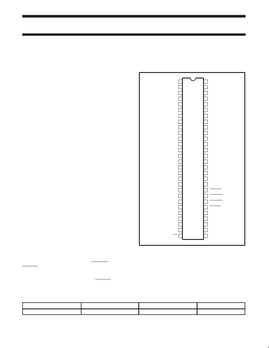
PIN CONFIGURATION
SW00892
1
2
3
4
5
6
7
8
9
10
11
12
45
46
47
48
49
50
51
52
53
54
55
56
VSS
REF1
VDD3V
XTAL_IN
XTAL_OUT
VSS
PCICLK_F
PCICLK1
VDD3V
PCICLK2
CPUCLK0
VSS
CPUCLK1
VDD3V
CPUCLK2
PCICLK3
13
14
15
16
17
18
39
40
41
42
43
44
VSS
PCICLK4
PCICLK5
VDD3V
PCICLK6
CPUCLK3
PCICLK7
19
38
VSS
20
21
22
23
24
25
32
33
34
35
36
37
VDD3V
3V66_0
3V66_1
SEL1
SEL0
VSS
26
31
27
30
48MHz_USB
28
29
SEl133/100
REF0
VSS
3V66_2
3V66_3
VDD3V
VDD25V
APIC2
APIC1
APIC0
VDD25V
CPUDIV2_1
CPUDIV2_0
VSS
VDD25V
VSS
VDD25V
VSS
PCISTOP
CPUSTOP
PWRDWN
SPREAD
VDD3V
VSS
ORDERING INFORMATION
PACKAGES
TEMPERATURE RANGE
ORDER CODE
DRAWING NUMBER
56-Pin plastic SSOP
0 to +70
°C
PCK2010RADL
SOT371-1
Intel and Pentium are registered trademarks of Intel Corporation.
相关PDF资料 |
PDF描述 |
|---|---|
| 935268676165 | LVC/LCX/Z SERIES, POSITIVE EDGE TRIGGERED D FLIP-FLOP, INVERTED OUTPUT, PDSO5 |
| 935268676115 | LVC/LCX/Z SERIES, POSITIVE EDGE TRIGGERED D FLIP-FLOP, INVERTED OUTPUT, PDSO5 |
| 935272023125 | LVC/LCX/Z SERIES, POSITIVE EDGE TRIGGERED D FLIP-FLOP, INVERTED OUTPUT, PDSO5 |
| 0802701R0 | TELEFON-AKKU |
| 935268720115 | LVC/LCX/Z SERIES, 1-BIT DRIVER, TRUE OUTPUT, PDSO5 |
相关代理商/技术参数 |
参数描述 |
|---|---|
| 935268721125 | 制造商:NXP Semiconductors 功能描述:Buffer/Line Driver 1-CH Non-Inverting 3-ST CMOS 5-Pin TSSOP T/R |
| 935269304128 | 制造商:ST-Ericsson 功能描述:IC AUDIO CODEC W/TCH SCRN 48LQFP |
| 935269544557 | 制造商:NXP Semiconductors 功能描述:SUB ONLY TDA9587-2US1-V1.3 |
| 935269987557 | 制造商:NXP Semiconductors 功能描述:SUB ONLY TDA9587-1US1-V1.8 SUBBED TO 935269987557 |
| 935270713557 | 制造商:NXP Semiconductors 功能描述:SUB ONLY IC CHP |
发布紧急采购,3分钟左右您将得到回复。