- 您现在的位置:买卖IC网 > PDF目录24830 > 935269451112 (NXP SEMICONDUCTORS) 133 MHz, PROC SPECIFIC CLOCK GENERATOR, PDSO56 PDF资料下载
参数资料
| 型号: | 935269451112 |
| 厂商: | NXP SEMICONDUCTORS |
| 元件分类: | 时钟产生/分配 |
| 英文描述: | 133 MHz, PROC SPECIFIC CLOCK GENERATOR, PDSO56 |
| 封装: | 7.50 MM, PLASTIC, MO-118, SOT-371-1, SSOP-56 |
| 文件页数: | 2/16页 |
| 文件大小: | 105K |
| 代理商: | 935269451112 |
Philips Semiconductors
Product specification
PCK2014A
CK98 (100/133 MHz) spread spectrum
system clock generator
2001 Apr 02
10
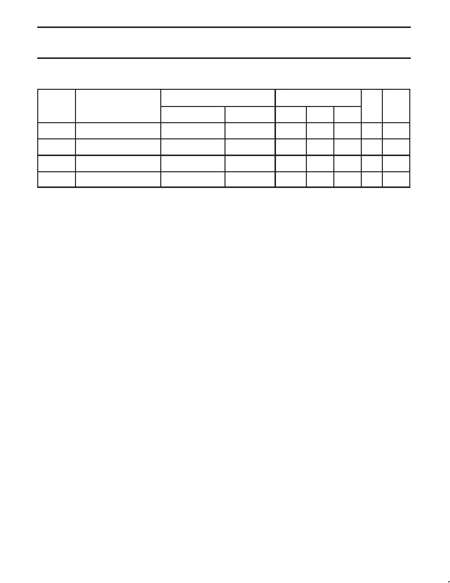
AC CHARACTERISTICS (Continued)
TEST CONDITIONS
LIMITS
SYMBOL
PARAMETER
TEST CONDITIONS
Tamb = 0 to +70 °C
UNIT
NOTES
SYMBOL
PARAMETER
Measurement loads
(lumped)
Measure points
MIN
TYP
MAX
UNIT
NOTES
THPOFFSET
CPUCLK to 3V66 CLK,
CPU leads
CPU@20 pF,
3V66@30 pF
CPU@1.25 V,
3V66@1.5 V
0.0
0.45
1.5
ns
1
THPOFFSET
3V66 CLK to PCI,
3V66 leads
3V66@30 pF,
PCI@30 pF
3V66@1.5 V,
PCI@1.5 V
1.5
2.0
3.5
ns
1
THPOFFSET
CPUCLK to APIC,
CPU leads
CPU@20 pF,
IOAPIC@20 pF
3CPU@1.25 V,
IOAPIC@1.25 V
1.5
2.4
4.0
ns
1
THPOFFSET
CPUCLK to PCI,
CPU leads
CPU@20 pF
PCI@30 pF
CPU@1.25 V
PCI@1.5 V
1.5
2.7
4.0
ns
NOTES:
1. Output drivers must have monotonic rise/fall times through the specified VOL/VOH levels.
2. Period, jitter, offset and skew measured on rising edge @1.25 V for 2.5 V clocks and @ 1.5 V for 3.3 V clocks.
3. The PCI is the CPUCLK divided by four at CPUCLK = 133 MHz. The 3V66 CLK is internal VCO frequency divided by three at
CPUCLK = 100 MHz.
4. 3V66 CLK is internal VCO frequency divided by two at CPUCLK = 133 MHz. The 3V66 CLK is internal VCO frequency divided by three at
CPUCLK = 100 MHz.
5. THKH is measured at 2.0 V for 2.5 V outputs, 2.4 V for 3.3 V outputs as shown in Figure 4.
6. THKL is measured at 0.4 V for all outputs as shown in Figure 4.
7. The time is specified from when VDDQ achieves its nominal operating level (typical condition VDDQ = 3.3 V) until the frequency output is
stable and operating within specification.
8. THRISE and THFALL are measured as a transition through the threshold region VOL = 0.4 V and VOH = 2.4 V for 3 V outputs, VOL = 0.4 V, and
VOH = 2.0 V for 2.5 V outputs. (1 mA) JEDEC specification.
9. The average period over any 1
s period of time must be greater than the minimum specified period.
10. Calculated at minimum edge-rate (1 V/ns) to guarantee 45/55% duty-cycle. Pulse width is required to be wider at faster edge-rate to ensure
duty-cycle specification is met.
11. Output (see Figure 5 for measure points).
相关PDF资料 |
PDF描述 |
|---|---|
| 0803-7700-03 | VDSL / PSTN CO Splitter |
| 935269471115 | 2.8 V FIXED POSITIVE LDO REGULATOR, 0.06 V DROPOUT, PDSO5 |
| 935269472115 | 3 V FIXED POSITIVE LDO REGULATOR, 0.06 V DROPOUT, PDSO5 |
| 935269473115 | 3.2 V FIXED POSITIVE LDO REGULATOR, 0.055 V DROPOUT, PDSO5 |
| 935269475115 | 5 V FIXED POSITIVE LDO REGULATOR, 0.04 V DROPOUT, PDSO5 |
相关代理商/技术参数 |
参数描述 |
|---|---|
| 935269544557 | 制造商:NXP Semiconductors 功能描述:SUB ONLY TDA9587-2US1-V1.3 |
| 935269987557 | 制造商:NXP Semiconductors 功能描述:SUB ONLY TDA9587-1US1-V1.8 SUBBED TO 935269987557 |
| 935270713557 | 制造商:NXP Semiconductors 功能描述:SUB ONLY IC CHP |
| 935270792551 | 制造商:NXP Semiconductors 功能描述:IC BUFF DVR TRI-ST 16BIT 56VFBGA |
| 935270792557 | 制造商:NXP Semiconductors 功能描述:IC BUFF DVR TRI-ST 16BIT 56VFBGA |
发布紧急采购,3分钟左右您将得到回复。