- 您现在的位置:买卖IC网 > PDF目录42457 > 93LC66A-I/SM 512 X 8 MICROWIRE BUS SERIAL EEPROM, PDSO8 PDF资料下载
参数资料
| 型号: | 93LC66A-I/SM |
| 元件分类: | PROM |
| 英文描述: | 512 X 8 MICROWIRE BUS SERIAL EEPROM, PDSO8 |
| 封装: | 0.208 INCH, PLASTIC, SOIC-8 |
| 文件页数: | 6/12页 |
| 文件大小: | 226K |
| 代理商: | 93LC66A-I/SM |
93LC66A/B
1998 Microchip Technology Inc.
DS21209C-page 3
2.0
PIN DESCRIPTION
2.1
Chip Select (CS)
A high level selects the device; a low level deselects the
device and forces it into standby mode. However, a pro-
gramming cycle which is already in progress will be
completed, regardless of the Chip Select (CS) input
signal. If CS is brought low during a program cycle, the
device will go into standby mode as soon as the pro-
gramming cycle is completed.
CS must be low for 250 ns minimum (TCSL) between
consecutive instructions. If CS is low, the internal con-
trol logic is held in a RESET status.
2.2
Serial Clock (CLK)
The Serial Clock (CLK) is used to synchronize the com-
munication between a master device and the 93LC66A/
B. Opcode, address, and data bits are clocked in on the
positive edge of CLK. Data bits are also clocked out on
the positive edge of CLK.
CLK can be stopped anywhere in the transmission
sequence (at high or low level) and can be continued
anytime with respect to clock high time (TCKH) and
clock low time (TCKL). This gives the controlling master
freedom in preparing opcode, address, and data.
CLK is a “Don't Care” if CS is low (device deselected).
If CS is high, but a START condition has not been
detected, any number of clock cycles can be received
by the device without changing its status (i.e., waiting
for a START condition).
CLK cycles are not required during the self-timed
WRITE (i.e., auto ERASE/WRITE) cycle.
After detection of a START condition the specified num-
ber of clock cycles (respectively low to high transitions
of CLK) must be provided. These clock cycles are
required to clock in all required opcode, address, and
data bits before an instruction is executed (Table 2-1
and Table 2-2). CLK and DI then become don't care
inputs waiting for a new START condition to be
detected.
2.3
Data In (DI)
Data In (DI) is used to clock in a START bit, opcode,
address, and data synchronously with the CLK input.
2.4
Data Out (DO)
Data Out (DO) is used in the READ mode to output
data synchronously with the CLK input (TPD after the
positive edge of CLK).
This pin also provides READY/BUSY status information
during ERASE and WRITE cycles. READY/BUSY sta-
tus information is available on the DO pin if CS is
brought high after being low for minimum chip select
low time (TCSL) and an ERASE or WRITE operation
has been initiated.
The status signal is not available on DO, if CS is held
low during the entire ERASE or WRITE cycle. In this
case, DO is in the HIGH-Z mode. If status is checked
after the ERASE/WRITE cycle, the data line will be high
to indicate the device is ready.
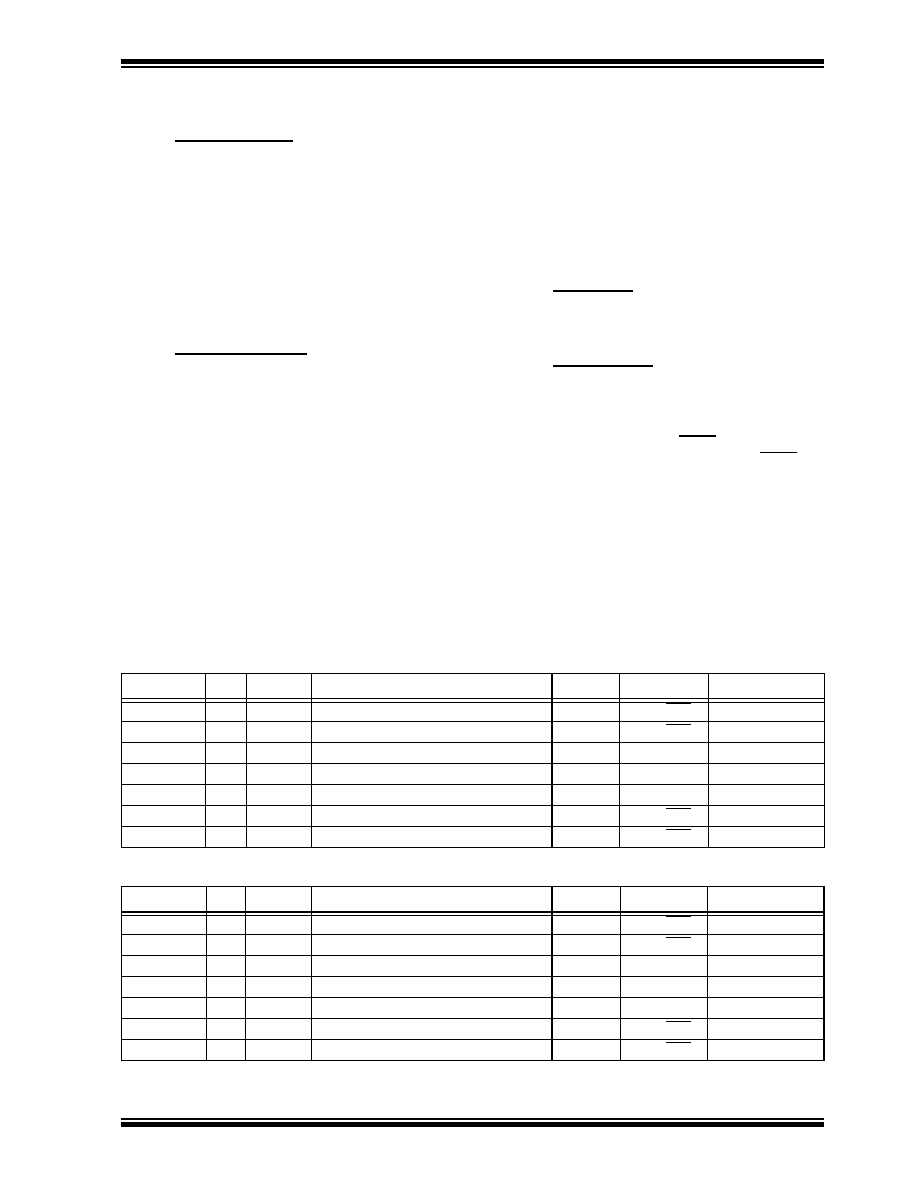
TABLE 2-1
INSTRUCTION SET FOR 93LC66A
Instruction
SB
Opcode
Address
Data In
Data Out
Req. CLK Cycles
ERASE
1
11
A8A7
A6A5A4A3
A2A1A0
—
(RDY/BSY)12
ERAL
1
00
1
0
X
XXXX
XX
—
(RDY/BSY)12
EWDS
1
00
0
X
XXXX
XX
—
HIGH-Z
12
EWEN
1
00
1
X
XXXX
XX
—
HIGH-Z
12
READ
1
10
A8A7
A6A5A4A3
A2A1A0
—
D7 - D0
20
WRITE
1
01
A8A7
A6A5A4A3
A2A1A0
D7 - D0
(RDY/BSY)20
WRAL
1
00
0
1
X
XXXX
XX
D7 - D0
(RDY/BSY)20
TABLE 2-2
INSTRUCTION SET FOR 93LC66B
Instruction
SB
Opcode
Address
Data In
Data Out
Req. CLK Cycles
ERASE
1
11
A7A6A5A4A3
A2A1A0
—
(RDY/BSY)11
ERAL
1
00
1
0
XXXX
XX
—
(RDY/BSY)11
EWDS
1
00
0
XXXX
XX
—
HIGH-Z
11
EWEN
1
00
1
XXXX
XX
—
HIGH-Z
11
READ
1
10
A7A6A5A4A3
A2A1A0
—
D15 - D0
27
WRITE
1
01
A7A6A5A4A3
A2A1A0
D15 - D0
(RDY/BSY)27
WRAL
1
00
0
1
XXXX
XX
D15 - D0
(RDY/BSY)27
相关PDF资料 |
PDF描述 |
|---|---|
| 93LC66BXT/SNJ22 | 256 X 16 MICROWIRE BUS SERIAL EEPROM, PDSO8 |
| 93LC66B/SM | 256 X 16 MICROWIRE BUS SERIAL EEPROM, PDSO8 |
| 93LC66B/PD22 | 256 X 16 MICROWIRE BUS SERIAL EEPROM, PDIP8 |
| 93LC66B/P | 256 X 16 MICROWIRE BUS SERIAL EEPROM, PDIP8 |
| 93LC66B/ST | 256 X 16 MICROWIRE BUS SERIAL EEPROM, PDSO8 |
相关代理商/技术参数 |
参数描述 |
|---|---|
| 93LC66AT/SN | 功能描述:电可擦除可编程只读存储器 512x8 RoHS:否 制造商:Atmel 存储容量:2 Kbit 组织:256 B x 8 数据保留:100 yr 最大时钟频率:1000 KHz 最大工作电流:6 uA 工作电源电压:1.7 V to 5.5 V 最大工作温度:+ 85 C 安装风格:SMD/SMT 封装 / 箱体:SOIC-8 |
| 93LC66AT/ST | 功能描述:电可擦除可编程只读存储器 512x8 RoHS:否 制造商:Atmel 存储容量:2 Kbit 组织:256 B x 8 数据保留:100 yr 最大时钟频率:1000 KHz 最大工作电流:6 uA 工作电源电压:1.7 V to 5.5 V 最大工作温度:+ 85 C 安装风格:SMD/SMT 封装 / 箱体:SOIC-8 |
| 93LC66AT-E/MNY | 功能描述:电可擦除可编程只读存储器 4K 512X8 SER EE,EXT RoHS:否 制造商:Atmel 存储容量:2 Kbit 组织:256 B x 8 数据保留:100 yr 最大时钟频率:1000 KHz 最大工作电流:6 uA 工作电源电压:1.7 V to 5.5 V 最大工作温度:+ 85 C 安装风格:SMD/SMT 封装 / 箱体:SOIC-8 |
| 93LC66AT-E/MS | 功能描述:电可擦除可编程只读存储器 512x8 RoHS:否 制造商:Atmel 存储容量:2 Kbit 组织:256 B x 8 数据保留:100 yr 最大时钟频率:1000 KHz 最大工作电流:6 uA 工作电源电压:1.7 V to 5.5 V 最大工作温度:+ 85 C 安装风格:SMD/SMT 封装 / 箱体:SOIC-8 |
| 93LC66AT-E/MSG | 功能描述:电可擦除可编程只读存储器 512x8 Lead Free Package RoHS:否 制造商:Atmel 存储容量:2 Kbit 组织:256 B x 8 数据保留:100 yr 最大时钟频率:1000 KHz 最大工作电流:6 uA 工作电源电压:1.7 V to 5.5 V 最大工作温度:+ 85 C 安装风格:SMD/SMT 封装 / 箱体:SOIC-8 |
发布紧急采购,3分钟左右您将得到回复。