- 您现在的位置:买卖IC网 > PDF目录360623 > 9403A (Fairchild Semiconductor Corporation) First-In First-Out (FIFO) Buffer Memory(先进先出缓冲器) PDF资料下载
参数资料
| 型号: | 9403A |
| 厂商: | Fairchild Semiconductor Corporation |
| 英文描述: | First-In First-Out (FIFO) Buffer Memory(先进先出缓冲器) |
| 中文描述: | 先入先出(FIFO)的缓冲存储器(先进先出缓冲器) |
| 文件页数: | 4/16页 |
| 文件大小: | 174K |
| 代理商: | 9403A |
www.fairchildsemi.com
4
9
Functional Description
(Continued)
Transfer to the Stack
—
The outputs of Flip-Flops F
0
-F
3
feed the stack. A LOW level on the TTS input initiates a
“
fall-through
”
action. If the top location of the stack is
empty, data is loaded into the stack and the input register is
re-initialized. Note that this initialization is postponed until
PL is LOW again. Thus, automatic FIFO action is achieved
by connecting the IRF output to the TTS input.
An RS Flip-Flop (the Request Initialization Flip-Flop shown
in Figure 10) in the control section records the fact that
data has been transferred to the stack. This prevents multi-
ple entry of the same word into the stack despite the fact
the IRF and TTS may still be LOW. The Request Initializa-
tion Flip-Flop is not cleared until PL goes LOW. Once in the
stack, data falls through the stack automatically, pausing
only when it is necessary to wait for an empty next location.
In the 9403A as in most modern FIFO designs, the MR
input only initializes the stack control section and does not
clear the data.
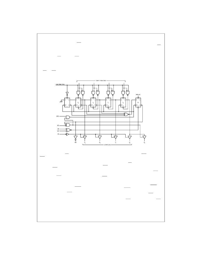
OUTPUT REGISTER (DATA EXTRACTION)
The Output Register receives 4-bit data words from the
bottom stack location, stores it and outputs data on a
3-STATE 4-bit parallel data bus or on a 3-STATE serial
data bus. The output section generates and receives the
necessary status and control signals. Figure 3 is a concep-
tual logic diagram of the output section.
FIGURE 3. Conceptual Output Section
Parallel Data Extraction
—
When the FIFO is empty after a
LOW pulse is applied to MR, the Output Register Empty
(ORE) output is LOW. After data has been entered into the
FIFO and has fallen through to the bottom stack location, it
is transferred into the Output Register provided the
“
Trans-
fer Out Parallel
”
(TOP) input is HIGH. As a result of the
data transfer ORE goes HIGH, indicating valid data on the
data outputs (provided the 3-STATE buffer is enabled).
TOP can now be used to clock out the next word. When
TOP goes LOW, ORE will go LOW indicating that the out-
put data has been extracted, but the data itself remains on
the output bus until the next HIGH level at TOP permits the
transfer of the next word (if available) into the Output Reg-
ister. During parallel data extraction CPSO should be LOW.
TOS should be grounded for single slice operation or con-
nected to the appropriate ORE for expanded operation
(see Expansion section).
TOP is not edge triggered. Therefore, if TOP goes HIGH
before data is available from the stack, but data does
become available before TOP goes LOW again, that data
will be transferred into the Output Register. However, inter-
nal control circuitry prevents the same data from being
transferred twice. If TOP goes HIGH and returns to LOW
before data is available from the stack, ORE remains LOW
indicating that there is no valid data at the outputs.
Serial Data Extraction
—
When the FIFO is empty after a
LOW pulse is applied to MR, the Output Register Empty
(ORE) output is LOW. After data has been entered into the
FIFO and has fallen through to the bottom stack location, it
is transferred into the Output Register provided TOS is
LOW and TOP is HIGH. As a result of the data transfer
ORE goes HIGH indicating valid data in the register. The
3-STATE Serial Data Output, Q
S
, is automatically enabled
and puts the first data bit on the output bus. Data is serially
shifted out on the HIGH-to-LOW transition of CPSO. To
prevent false shifting, CPSO should be LOW when the new
word is being loaded into the Output Register. The fourth
transition empties the shift register, forces ORE output
LOW and disables the serial output, Q
S
(refer to Figure 3).
For serial operation the ORE output may be tied to the TOS
input, requesting a new word from the stack as soon as the
previous one has been shifted out.
相关PDF资料 |
PDF描述 |
|---|---|
| 9405 | SORTIMENTSKOFFER SCHWARZ PVC |
| 940LB7C | FLUX LED SPECIFICATION |
| 940MR2C | FLUX LED SPECIFICATION |
| 940MW7C | FLUX LED SPECIFICATION |
| 940MY8C | FLUX LED SPECIFICATION |
相关代理商/技术参数 |
参数描述 |
|---|---|
| 9403A WAF | 制造商:Fairchild Semiconductor Corporation 功能描述: |
| 9403ADMQB | 制造商:未知厂家 制造商全称:未知厂家 功能描述:Multi-Mode FIFO |
| 9403ADMQB | 制造商:National Semiconductor Corporation 功能描述:FIFO Register Single 4-CH 24-Pin CDIP 制造商:National Semiconductor 功能描述:FIFO Register Single 4-CH 24-Pin CDIP |
| 9403ALMQB | 制造商:未知厂家 制造商全称:未知厂家 功能描述:Multi-Mode FIFO |
| 9403APC | 功能描述:寄存器 FIFO Buffer Memory RoHS:否 制造商:NXP Semiconductors 逻辑类型:CMOS 逻辑系列:HC 电路数量:1 最大时钟频率:36 MHz 传播延迟时间: 高电平输出电流:- 7.8 mA 低电平输出电流:7.8 mA 电源电压-最大:6 V 最大工作温度:+ 125 C 封装 / 箱体:SOT-38 封装:Tube |
发布紧急采购,3分钟左右您将得到回复。