- 您现在的位置:买卖IC网 > PDF目录25563 > 9DB1233AGLF (INTEGRATED DEVICE TECHNOLOGY INC) 9DB SERIES, PLL BASED CLOCK DRIVER, 12 TRUE OUTPUT(S), 0 INVERTED OUTPUT(S), PDSO64 PDF资料下载
参数资料
| 型号: | 9DB1233AGLF |
| 厂商: | INTEGRATED DEVICE TECHNOLOGY INC |
| 元件分类: | 时钟及定时 |
| 英文描述: | 9DB SERIES, PLL BASED CLOCK DRIVER, 12 TRUE OUTPUT(S), 0 INVERTED OUTPUT(S), PDSO64 |
| 封装: | 6.10 MM, 0.50 MM PITCH, ROHS COMPLIANT, MO-153, TSSOP-64 |
| 文件页数: | 4/15页 |
| 文件大小: | 181K |
| 代理商: | 9DB1233AGLF |
IDT Twelve Output Differential Buffer for PCIe Gen3
9DB1233
Twelve Output Differential Buffer for PCIe Gen3
12
1675B—11/08/10
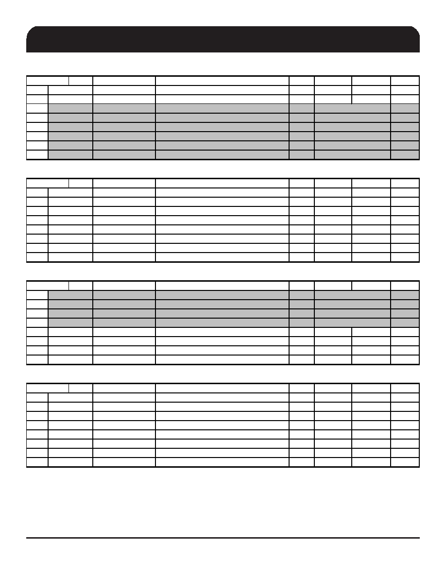
SMBus Table: Frequency Select Register
Pin #
Name
Control Function
Type
0
1
Default
Bit 7
HIGH_BW#
High or Low BW
RW
High BW
Low BW
Latch
Bit 6
BYPASS#/PLL
Bypass (non-PLL Mode) or PLL Mode
RW
Bypass
PLL
Latch
Bit 5
Reserved
RW
X
Bit 4
Reserved
RW
X
Bit 3
Reserved
RW
X
Bit 2
Reserved
RW
1
Bit 1
Reserved
RW
0
Bit 0
Reserved
RW
1
SMBus Table: Output Control Register
Pin #
Name
Control Function
Type
0
1
Default
Bit 7
DIF_7
Output Control (Disable = Hi-Z)
RW
Disable
Enable
1
Bit 6
DIF_6
Output Control (Disable = Hi-Z)
RW
Disable
Enable
1
Bit 5
DIF_5
Output Control (Disable = Hi-Z)
RW
Disable
Enable
1
Bit 4
DIF_4
Output Control (Disable = Hi-Z)
RW
Disable
Enable
1
Bit 3
DIF_3
Output Control (Disable = Hi-Z)
RW
Disable
Enable
1
Bit 2
DIF_2
Output Control (Disable = Hi-Z)
RW
Disable
Enable
1
Bit 1
DIF_1
Output Control (Disable = Hi-Z)
RW
Disable
Enable
1
Bit 0
DIF_0
Output Control (Disable = Hi-Z)
RW
Disable
Enable
1
SMBus Table: Output Control Register
Pin #
Name
Control Function
Type
0
1
Default
Bit 7
Reserved
RW
0
Bit 6
Reserved
RW
0
Bit 5
Reserved
RW
0
Bit 4
Reserved
RW
0
Bit 3
DIF_11
Output Control (Disable = Hi-Z)
RW
Disable
Enable
1
Bit 2
DIF_10
Output Control (Disable = Hi-Z)
RW
Disable
Enable
1
Bit 1
DIF_9
Output Control (Disable = Hi-Z)
RW
Disable
Enable
1
Bit 0
DIF_8
Output Control (Disable = Hi-Z)
RW
Disable
Enable
1
SMBus Table: Output Enable Readback
Pin #
Name
Control Function
Type
0
1
Default
Bit 7
OE7#
OE# Pin Readback
R
Enabled
Disabled
X
Bit 6
OE6#
OE# Pin Readback
R
Enabled
Disabled
X
Bit 5
OE5#
OE# Pin Readback
R
Enabled
Disabled
X
Bit 4
OE4#
OE# Pin Readback
R
Enabled
Disabled
X
Bit 3
OE3#
OE# Pin Readback
R
Enabled
Disabled
X
Bit 2
OE2#
OE# Pin Readback
R
Enabled
Disabled
X
Bit 1
OE1#
OE# Pin Readback
R
Enabled
Disabled
X
Bit 0
OE0#
OE# Pin Readback
R
Enabled
Disabled
X
-
Reserved
Byte 0
-
Reserved
-
Reserved
-
Reserved
Byte 1
43,42
38,37
27,28
22,23
19,20
14,15
11,12
6,7
Byte 2
-
58,59
53,54
38,37
50,51
45,46
Byte 3
43,42
27,28
22,23
19,20
14,15
11,12
Reserved
6,7
相关PDF资料 |
PDF描述 |
|---|---|
| 9DB1904BKLFT | 9DB SERIES, PLL BASED CLOCK DRIVER, 19 TRUE OUTPUT(S), 0 INVERTED OUTPUT(S), PQCC72 |
| 9DB1933AKLF | 9DB SERIES, PLL BASED CLOCK DRIVER, 19 TRUE OUTPUT(S), 0 INVERTED OUTPUT(S), PQCC72 |
| 9DB1933AKLFT | 9DB SERIES, PLL BASED CLOCK DRIVER, 19 TRUE OUTPUT(S), 0 INVERTED OUTPUT(S), PQCC72 |
| 9DB202CGLF | 9DB SERIES, PLL BASED CLOCK DRIVER, 2 TRUE OUTPUT(S), 0 INVERTED OUTPUT(S), PDSO20 |
| 9DB202CFLF | 9DB SERIES, PLL BASED CLOCK DRIVER, 2 TRUE OUTPUT(S), 0 INVERTED OUTPUT(S), PDSO20 |
相关代理商/技术参数 |
参数描述 |
|---|---|
| 9DB1233AGLFT | 功能描述:时钟缓冲器 12 OUTPUT PCIE GEN3 BUFFER RoHS:否 制造商:Texas Instruments 输出端数量:5 最大输入频率:40 MHz 传播延迟(最大值): 电源电压-最大:3.45 V 电源电压-最小:2.375 V 最大功率耗散: 最大工作温度:+ 85 C 最小工作温度:- 40 C 封装 / 箱体:LLP-24 封装:Reel |
| 9DB1904B | 制造商:IDT 制造商全称:Integrated Device Technology 功能描述:19 Output Differential Buffer for PCIe Gen2 and QPI |
| 9DB1904BKLF | 功能描述:时钟缓冲器 19 OUTPUT PCIE GEN2 BUFFER w/QPI RoHS:否 制造商:Texas Instruments 输出端数量:5 最大输入频率:40 MHz 传播延迟(最大值): 电源电压-最大:3.45 V 电源电压-最小:2.375 V 最大功率耗散: 最大工作温度:+ 85 C 最小工作温度:- 40 C 封装 / 箱体:LLP-24 封装:Reel |
| 9DB1904BKLFT | 功能描述:时钟缓冲器 19 OUTPUT PCIE GEN2 BUFFER w/QPI RoHS:否 制造商:Texas Instruments 输出端数量:5 最大输入频率:40 MHz 传播延迟(最大值): 电源电压-最大:3.45 V 电源电压-最小:2.375 V 最大功率耗散: 最大工作温度:+ 85 C 最小工作温度:- 40 C 封装 / 箱体:LLP-24 封装:Reel |
| 9DB1933 | 制造商:IDT 制造商全称:Integrated Device Technology 功能描述:Nineteen Output Differential Buffer for PCIe Gen3 |
发布紧急采购,3分钟左右您将得到回复。