- 您现在的位置:买卖IC网 > PDF目录25564 > 9DB306BL (INTEGRATED DEVICE TECHNOLOGY INC) 9DB SERIES, PLL BASED CLOCK DRIVER, 6 TRUE OUTPUT(S), 0 INVERTED OUTPUT(S), PDSO28 PDF资料下载
参数资料
| 型号: | 9DB306BL |
| 厂商: | INTEGRATED DEVICE TECHNOLOGY INC |
| 元件分类: | 时钟及定时 |
| 英文描述: | 9DB SERIES, PLL BASED CLOCK DRIVER, 6 TRUE OUTPUT(S), 0 INVERTED OUTPUT(S), PDSO28 |
| 封装: | 4.40 X 9.70 MM, 0.925 MM HEIGHT, TSSOP-28 |
| 文件页数: | 15/17页 |
| 文件大小: | 268K |
| 代理商: | 9DB306BL |
ICS9DB306BL REVISION C AUGUST 13, 2009
7
2009 Integrated Device Technology, Inc.
ICS9DB306 Data Sheet
PCI EXPRESS JITTER ATTENUATOR
APPLICATION INFORMATION
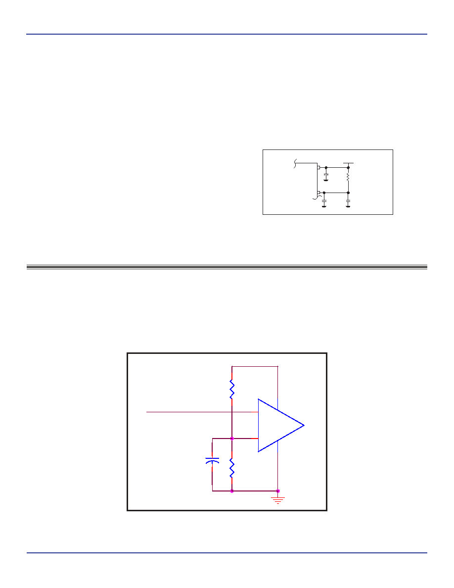
Figure 2 shows how the differential input can be wired to accept
single ended levels. The reference voltage V_REF = V
DD
/2 is
generated by the bias resistors R1, R2 and C1. This bias circuit
should be located as close as possible to the input pin. The ratio
FIGURE 2. SINGLE ENDED SIGNAL DRIVING DIFFERENTIAL INPUT
WIRING THE DIFFERENTIAL INPUT TO ACCEPT SINGLE ENDED LEVELS
of R1 and R2 might need to be adjusted to position the V_REF in
the center of the input voltage swing. For example, if the input
clock swing is only 2.5V and V
CC
= 3.3V, V_REF should be 1.25V
and R2/R1 = 0.609.
FIGURE 1. POWER SUPPLY FILTERING
V_REF
R1
1K
C1
0.1u
R2
1K
Single Ended Clock Input
CLKx
nCLKx
VCC
POWER SUPPLY FILTERING TECHNIQUES
As in any high speed analog circuitry, the power supply pins are
vulnerable to random noise. To achieve optimum jitter perfor-
mance, power supply isolation is required. The ICS9DB306 pro-
vides separate power supplies to isolate any high switching noise
from the outputs to the internal PLL. V
CC and VCCA should be indi-
vidually connected to the power supply plane through vias, and
0.01F bypass capacitors should be used for each pin.
Figure 1
illustrates this for a generic V
CC pin and also shows that VCCA
requires that an additional 24
Ω resistor along with a 10F by-
pass capacitor be connected to the V
CCA pin.
VCC
VCCA
3.3V
24
Ω
10F
.01F
相关PDF资料 |
PDF描述 |
|---|---|
| 9DB401BGLFT | 9DB SERIES, PLL BASED CLOCK DRIVER, 4 TRUE OUTPUT(S), 0 INVERTED OUTPUT(S), PDSO28 |
| 9DB401BFLFT | 9DB SERIES, PLL BASED CLOCK DRIVER, 4 TRUE OUTPUT(S), 0 INVERTED OUTPUT(S), PDSO28 |
| 9DB401CGLFT | 9DB SERIES, PLL BASED CLOCK DRIVER, 4 TRUE OUTPUT(S), 0 INVERTED OUTPUT(S), PDSO28 |
| 9DB401CFLF | 9DB SERIES, PLL BASED CLOCK DRIVER, 4 TRUE OUTPUT(S), 0 INVERTED OUTPUT(S), PDSO28 |
| 9DB403DGILFT | 9DB SERIES, PLL BASED CLOCK DRIVER, 4 TRUE OUTPUT(S), 0 INVERTED OUTPUT(S), PDSO28 |
相关代理商/技术参数 |
参数描述 |
|---|---|
| 9DB306BLI | 制造商:Integrated Device Technology Inc 功能描述:ZERO DLY PLL CLOCK BFFR SGL 28TSSOP - Rail/Tube |
| 9DB306BLILF | 功能描述:IC JITTER ATTENUATOR 28-TSSOP 制造商:idt, integrated device technology inc 系列:- 包装:管件 零件状态:过期 PLL:是 主要用途:PCI Express(PCIe) 输入:HCSL,LVDS,LVHSTL,LVPECL,SSTL 输出:LVPECL 电路数:1 比率 - 输入:输出:1:6 差分 - 输入:输出:是/是 频率 - 最大值:140MHz 电压 - 电源:2.97 V ~ 3.63 V 工作温度:-40°C ~ 85°C 安装类型:表面贴装 封装/外壳:28-TSSOP(0.173",4.40mm 宽) 供应商器件封装:28-TSSOP 标准包装:50 |
| 9DB306BLILFT | 功能描述:IC JITTER ATTENUATOR 28-TSSOP 制造商:idt, integrated device technology inc 系列:- 包装:带卷(TR) 零件状态:过期 PLL:是 主要用途:PCI Express(PCIe) 输入:HCSL,LVDS,LVHSTL,LVPECL,SSTL 输出:LVPECL 电路数:1 比率 - 输入:输出:1:6 差分 - 输入:输出:是/是 频率 - 最大值:140MHz 电压 - 电源:2.97 V ~ 3.63 V 工作温度:-40°C ~ 85°C 安装类型:表面贴装 封装/外壳:28-TSSOP(0.173",4.40mm 宽) 供应商器件封装:28-TSSOP 标准包装:1,000 |
| 9DB306BLIT | 制造商:Integrated Device Technology Inc 功能描述:ZERO DLY PLL CLOCK BFFR SGL 28TSSOP - Rail/Tube |
| 9DB306BLLF | 功能描述:时钟合成器/抖动清除器 2 LVPECL Output PCI- Express Buffer RoHS:否 制造商:Skyworks Solutions, Inc. 输出端数量: 输出电平: 最大输出频率: 输入电平: 最大输入频率:6.1 GHz 电源电压-最大:3.3 V 电源电压-最小:2.7 V 封装 / 箱体:TSSOP-28 封装:Reel |
发布紧急采购,3分钟左右您将得到回复。