- 您现在的位置:买卖IC网 > PDF目录25564 > 9DB401CGLFT (INTEGRATED DEVICE TECHNOLOGY INC) 9DB SERIES, PLL BASED CLOCK DRIVER, 4 TRUE OUTPUT(S), 0 INVERTED OUTPUT(S), PDSO28 PDF资料下载
参数资料
| 型号: | 9DB401CGLFT |
| 厂商: | INTEGRATED DEVICE TECHNOLOGY INC |
| 元件分类: | 时钟及定时 |
| 英文描述: | 9DB SERIES, PLL BASED CLOCK DRIVER, 4 TRUE OUTPUT(S), 0 INVERTED OUTPUT(S), PDSO28 |
| 封装: | 4.40 MM, 0.65 MM PITCH, ROHS COMPLIANT, MO-153, TSSOP-28 |
| 文件页数: | 17/17页 |
| 文件大小: | 160K |
| 代理商: | 9DB401CGLFT |
IDT
Four Output Differential Buffer for PCI Express
9DB401C
REV H 01/27/11
9DB401C
Four Output Differential Buffer for PCI Express
9
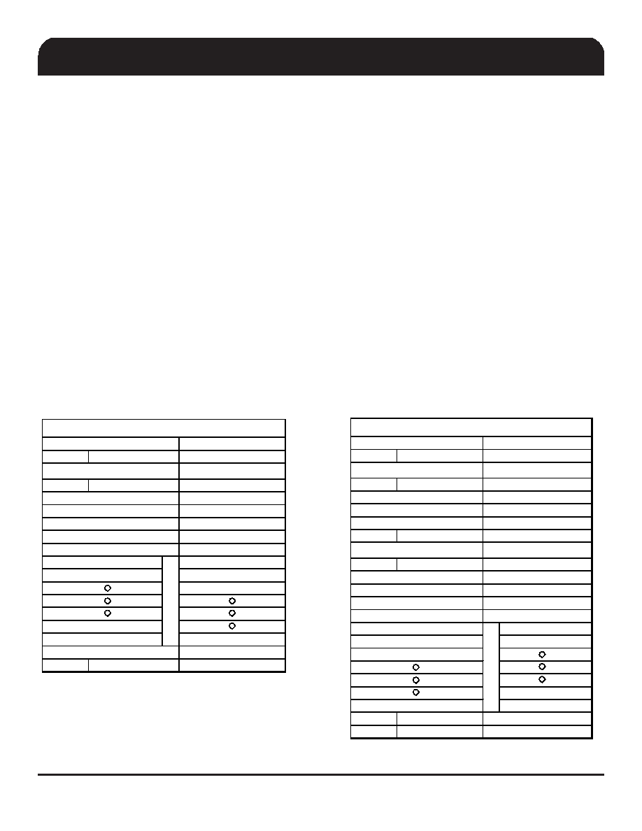
General SMBus serial interface information for the 9DB401C
How to Write:
Controller (host) sends a start bit.
Controller (host) sends the write address DC
(h)
IDT clock will
acknowledge
Controller (host) sends the begining byte location = N
IDT clock will
acknowledge
Controller (host) sends the data byte count = X
IDT clock will
acknowledge
Controller (host) starts sending
Byte N through
Byte N + X -1
IDT clock will
acknowledge each byte one at a time
Controller (host) sends a Stop bit
How to Read:
Controller (host) will send start bit.
Controller (host) sends the write address DC
(h)
IDT clock will
acknowledge
Controller (host) sends the begining byte
location = N
IDT clock will
acknowledge
Controller (host) will send a separate start bit.
Controller (host) sends the read address DD
(h)
IDT clock will
acknowledge
IDT clock will send the data byte count = X
IDT clock sends
Byte N + X -1
IDT clock sends
Byte 0 through byte X (if X
(h)
was written to byte 8).
Controller (host) will need to acknowledge each byte
Controllor (host) will send a not acknowledge bit
Controller (host) will send a stop bit
IDT (Slave/Receiver)
T
WR
ACK
P
Byte N + X - 1
Data Byte Count = X
Beginning Byte N
stoP bit
X
By
te
Index Block Write Operation
Slave Address DC(h)
Beginning Byte = N
WRite
starT bit
Controller (Host)
T
starT bit
WR
WRite
RT
Repeat starT
RD
ReaD
Beginning Byte N
Byte N + X - 1
N
Not acknowledge
PstoP bit
IDT (Slave/Receiver)
Controller (Host)
X
By
te
ACK
Data Byte Count = X
ACK
Slave Address DD(h)
Index Block Read Operation
Slave Address DC(h)
Beginning Byte = N
ACK
相关PDF资料 |
PDF描述 |
|---|---|
| 9DB401CFLF | 9DB SERIES, PLL BASED CLOCK DRIVER, 4 TRUE OUTPUT(S), 0 INVERTED OUTPUT(S), PDSO28 |
| 9DB403DGILFT | 9DB SERIES, PLL BASED CLOCK DRIVER, 4 TRUE OUTPUT(S), 0 INVERTED OUTPUT(S), PDSO28 |
| 9DB403DFILFT | 9DB SERIES, PLL BASED CLOCK DRIVER, 4 TRUE OUTPUT(S), 0 INVERTED OUTPUT(S), PDSO28 |
| 9DB403DFILF | 9DB SERIES, PLL BASED CLOCK DRIVER, 4 TRUE OUTPUT(S), 0 INVERTED OUTPUT(S), PDSO28 |
| 9DB403DGLF | 9DB SERIES, PLL BASED CLOCK DRIVER, 4 TRUE OUTPUT(S), 0 INVERTED OUTPUT(S), PDSO28 |
相关代理商/技术参数 |
参数描述 |
|---|---|
| 9DB403DFILF | 功能描述:时钟缓冲器 4 OUTPUT PCIE GEN1 BUFFER RoHS:否 制造商:Texas Instruments 输出端数量:5 最大输入频率:40 MHz 传播延迟(最大值): 电源电压-最大:3.45 V 电源电压-最小:2.375 V 最大功率耗散: 最大工作温度:+ 85 C 最小工作温度:- 40 C 封装 / 箱体:LLP-24 封装:Reel |
| 9DB403DFILFT | 功能描述:时钟缓冲器 4 OUTPUT PCIE GEN1 BUFFER RoHS:否 制造商:Texas Instruments 输出端数量:5 最大输入频率:40 MHz 传播延迟(最大值): 电源电压-最大:3.45 V 电源电压-最小:2.375 V 最大功率耗散: 最大工作温度:+ 85 C 最小工作温度:- 40 C 封装 / 箱体:LLP-24 封装:Reel |
| 9DB403DFLF | 功能描述:时钟缓冲器 4 OUTPUT PCIE GEN1 BUFFER RoHS:否 制造商:Texas Instruments 输出端数量:5 最大输入频率:40 MHz 传播延迟(最大值): 电源电压-最大:3.45 V 电源电压-最小:2.375 V 最大功率耗散: 最大工作温度:+ 85 C 最小工作温度:- 40 C 封装 / 箱体:LLP-24 封装:Reel |
| 9DB403DFLFT | 功能描述:时钟缓冲器 4 OUTPUT PCIE GEN1 BUFFER RoHS:否 制造商:Texas Instruments 输出端数量:5 最大输入频率:40 MHz 传播延迟(最大值): 电源电压-最大:3.45 V 电源电压-最小:2.375 V 最大功率耗散: 最大工作温度:+ 85 C 最小工作温度:- 40 C 封装 / 箱体:LLP-24 封装:Reel |
| 9DB403DGILF | 功能描述:时钟缓冲器 4 OUTPUT PCIE GEN1 BUFFER RoHS:否 制造商:Texas Instruments 输出端数量:5 最大输入频率:40 MHz 传播延迟(最大值): 电源电压-最大:3.45 V 电源电压-最小:2.375 V 最大功率耗散: 最大工作温度:+ 85 C 最小工作温度:- 40 C 封装 / 箱体:LLP-24 封装:Reel |
发布紧急采购,3分钟左右您将得到回复。