- 您现在的位置:买卖IC网 > PDF目录25564 > 9DB401CGLFT (INTEGRATED DEVICE TECHNOLOGY INC) 9DB SERIES, PLL BASED CLOCK DRIVER, 4 TRUE OUTPUT(S), 0 INVERTED OUTPUT(S), PDSO28 PDF资料下载
参数资料
| 型号: | 9DB401CGLFT |
| 厂商: | INTEGRATED DEVICE TECHNOLOGY INC |
| 元件分类: | 时钟及定时 |
| 英文描述: | 9DB SERIES, PLL BASED CLOCK DRIVER, 4 TRUE OUTPUT(S), 0 INVERTED OUTPUT(S), PDSO28 |
| 封装: | 4.40 MM, 0.65 MM PITCH, ROHS COMPLIANT, MO-153, TSSOP-28 |
| 文件页数: | 9/17页 |
| 文件大小: | 160K |
| 代理商: | 9DB401CGLFT |
9DB401C
Four Output Differential Buffer for PCI Express
17
Innovate with IDT and accelerate your future networks. Contact:
www.IDT.com
For Sales
800-345-7015
408-284-8200
Fax: 408-284-2775
For Tech Support
408-284-6578
pcclockhelp@idt.com
Corporate Headquarters
Integrated Device Technology, Inc.
6024 Silver Creek Valley Road
San Jose, CA 95138
United States
800 345 7015
+408 284 8200 (outside U.S.)
Asia Pacific and Japan
IDT Singapore Pte. Ltd.
1 Kallang Sector #07-01/06
KolamAyer Industrial Park
Singapore 349276
Phone: 65-6-744-3356
Fax: 65-6-744-1764
Europe
IDT Europe Limited
321 Kingston Road
Leatherhead, Surrey
KT22 7TU
England
Phone: 44-1372-363339
Fax: 44-1372-378851
2010 Integrated Device Technology, Inc. All rights reserved. Product specifications subject to change without notice. IDT and the IDT logo are trademarks
of Integrated Device Technology, Inc. Accelerated Thinking is a service mark of Integrated Device Technology, Inc. All other brands, product names and marks
are or may be trademarks or registered trademarks used to identify products or services of their respective owners.
Printed in USA
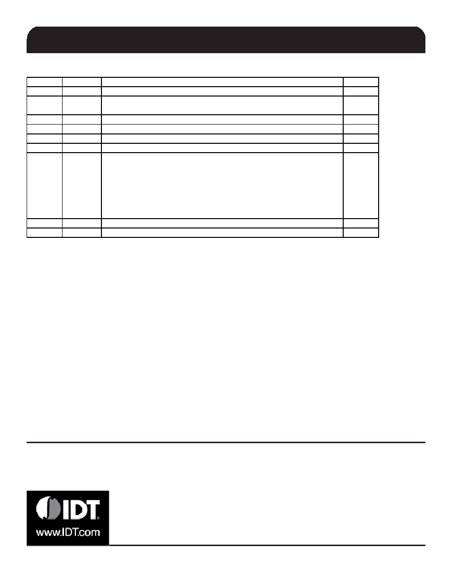
Revision History
Rev.
Issue Date Description
Page #
0.1
4/21/2005 Changed Ordering Information from"LN" to "LF".
14,15
A
8/15/2005
1. Updated LF Ordering Information to RoHS Compliant.
2. Release to web.
14-15
B
9/7/2006
Updated Electrical Characteristics.
Various
C
5/22/2007 Updated Polarity Inversion Table.
2
D
2/28/2008 Added Input Clock Specs
6
E
3/18/2008 Fixed typo in clock Input Parameters
6
F
9/5/2008
1. Updated Electrical Characteristics to add propagation delay and phase
noise information.
2. Added SMBus electrical characteristics
3. Added foot note about DIF input running in order for the SMBus
interface to work
4. Added foot note to Byte 1 about functionality of OE bits and OE pins.
5. Updated Block Diagram to correctly indicate the OE pins.
Various
G
11/18/2010 Updated Block Diagram
1
H
1/27/2011 Updated Termination Figure 4
8
相关PDF资料 |
PDF描述 |
|---|---|
| 9DB401CFLF | 9DB SERIES, PLL BASED CLOCK DRIVER, 4 TRUE OUTPUT(S), 0 INVERTED OUTPUT(S), PDSO28 |
| 9DB403DGILFT | 9DB SERIES, PLL BASED CLOCK DRIVER, 4 TRUE OUTPUT(S), 0 INVERTED OUTPUT(S), PDSO28 |
| 9DB403DFILFT | 9DB SERIES, PLL BASED CLOCK DRIVER, 4 TRUE OUTPUT(S), 0 INVERTED OUTPUT(S), PDSO28 |
| 9DB403DFILF | 9DB SERIES, PLL BASED CLOCK DRIVER, 4 TRUE OUTPUT(S), 0 INVERTED OUTPUT(S), PDSO28 |
| 9DB403DGLF | 9DB SERIES, PLL BASED CLOCK DRIVER, 4 TRUE OUTPUT(S), 0 INVERTED OUTPUT(S), PDSO28 |
相关代理商/技术参数 |
参数描述 |
|---|---|
| 9DB403DFILF | 功能描述:时钟缓冲器 4 OUTPUT PCIE GEN1 BUFFER RoHS:否 制造商:Texas Instruments 输出端数量:5 最大输入频率:40 MHz 传播延迟(最大值): 电源电压-最大:3.45 V 电源电压-最小:2.375 V 最大功率耗散: 最大工作温度:+ 85 C 最小工作温度:- 40 C 封装 / 箱体:LLP-24 封装:Reel |
| 9DB403DFILFT | 功能描述:时钟缓冲器 4 OUTPUT PCIE GEN1 BUFFER RoHS:否 制造商:Texas Instruments 输出端数量:5 最大输入频率:40 MHz 传播延迟(最大值): 电源电压-最大:3.45 V 电源电压-最小:2.375 V 最大功率耗散: 最大工作温度:+ 85 C 最小工作温度:- 40 C 封装 / 箱体:LLP-24 封装:Reel |
| 9DB403DFLF | 功能描述:时钟缓冲器 4 OUTPUT PCIE GEN1 BUFFER RoHS:否 制造商:Texas Instruments 输出端数量:5 最大输入频率:40 MHz 传播延迟(最大值): 电源电压-最大:3.45 V 电源电压-最小:2.375 V 最大功率耗散: 最大工作温度:+ 85 C 最小工作温度:- 40 C 封装 / 箱体:LLP-24 封装:Reel |
| 9DB403DFLFT | 功能描述:时钟缓冲器 4 OUTPUT PCIE GEN1 BUFFER RoHS:否 制造商:Texas Instruments 输出端数量:5 最大输入频率:40 MHz 传播延迟(最大值): 电源电压-最大:3.45 V 电源电压-最小:2.375 V 最大功率耗散: 最大工作温度:+ 85 C 最小工作温度:- 40 C 封装 / 箱体:LLP-24 封装:Reel |
| 9DB403DGILF | 功能描述:时钟缓冲器 4 OUTPUT PCIE GEN1 BUFFER RoHS:否 制造商:Texas Instruments 输出端数量:5 最大输入频率:40 MHz 传播延迟(最大值): 电源电压-最大:3.45 V 电源电压-最小:2.375 V 最大功率耗散: 最大工作温度:+ 85 C 最小工作温度:- 40 C 封装 / 箱体:LLP-24 封装:Reel |
发布紧急采购,3分钟左右您将得到回复。