- 您现在的位置:买卖IC网 > PDF目录25564 > 9DB633AGLFT (INTEGRATED DEVICE TECHNOLOGY INC) 9DB SERIES, PLL BASED CLOCK DRIVER, 6 TRUE OUTPUT(S), 0 INVERTED OUTPUT(S), PDSO28 PDF资料下载
参数资料
| 型号: | 9DB633AGLFT |
| 厂商: | INTEGRATED DEVICE TECHNOLOGY INC |
| 元件分类: | 时钟及定时 |
| 英文描述: | 9DB SERIES, PLL BASED CLOCK DRIVER, 6 TRUE OUTPUT(S), 0 INVERTED OUTPUT(S), PDSO28 |
| 封装: | 4.40 MM, 0.65 MM PITCH, ROHS COMPLIANT, MO-153, TSSOP-28 |
| 文件页数: | 10/14页 |
| 文件大小: | 182K |
| 代理商: | 9DB633AGLFT |
IDT
Six Output Differential Buffer for PCIe Gen3
1668C—04/20/11
9DB633
Six Output Differential Buffer for PCIe Gen3
5
Datasheet
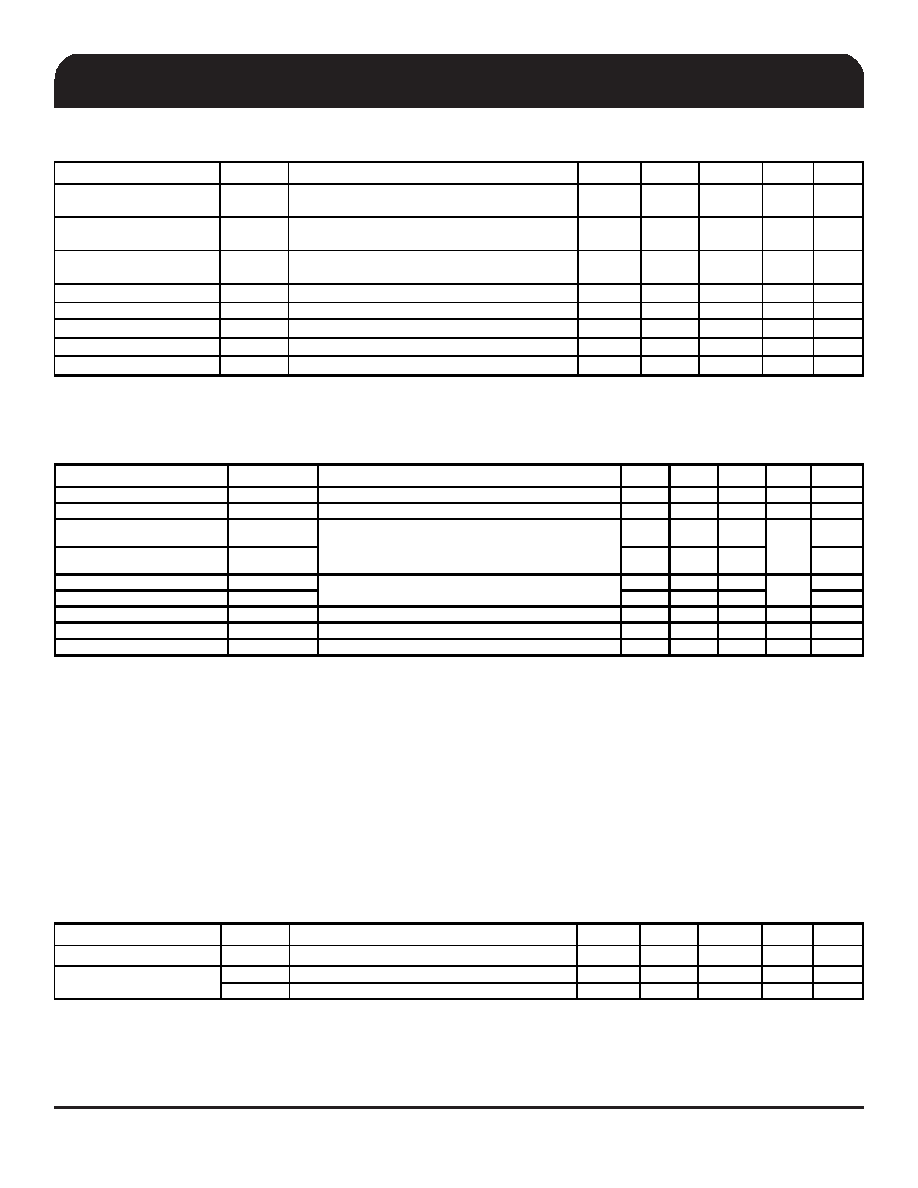
Electrical Characteristics - Clock Input Parameters
TA = TCOM or TIND; Supply Voltage VDD = 3.3 V +/-5%
PARAMETER
SYMBOL
CONDITIONS
MIN
TYP
MAX
UNITS NOTES
Input High Voltage - DIF_IN
VIHDIF
Differential inputs
(single-ended measurement)
600
800
1150
mV
1
Input Low Voltage - DIF_IN
VILDIF
Differential inputs
(single-ended measurement)
VSS - 300
0
300
mV
1
Input Common Mode
Voltage - DIF_IN
VCOM
Common Mode Input Voltage
300
1000
mV
1
Input Amplitude - DIF_IN
VSWING
Peak to Peak value
300
1450
mV
1
Input Slew Rate - DIF_IN
dv/dt
Measured differentially
0.4
8
V/ns
1,2
Input Leakage Current
IIN
VIN = VDD , VIN = GND
-5
5
uA
1
Input Duty Cycle
dtin
Measurement from differential wavefrom
45
55
%
1
Input Jitter - Cycle to Cycle
JDIFIn
Differential Measurement
0
125
ps
1
1 Guaranteed by design and characterization, not 100% tested in production.
2Slew rate measured through +/-75mV window centered around differential zero
Electrical Characteristics - DIF 0.7V Current Mode Differential Outputs
TA = TCOM or TIND; Supply Voltage VDD = 3.3 V +/-5%
PARAMETER
SYMBOL
CONDITIONS
MIN
TYP
MAX
UNITS NOTES
Slew rate
Trf
Scope averaging on
0.6
2.5
4
V/ns
1, 2, 3
Slew rate matching
ΔTrf
Slew rate matching, Scope averaging on
9.5
20
%
1, 2, 4
Voltage High
VHigh
660
740
850
1
Voltage Low
VLow
-150
8
150
1
Max Voltage
Vmax
760
1150
1
Min VoltageVmin
-300
-3
1
Vswing
Scope averaging off
300
1506
mV
1, 2
Crossing Voltage (abs)
Vcross_abs
Scope averaging off
250
378
550
mV
1, 5
Crossing Voltage (var)
Δ-Vcross
Scope averaging off
54
140
mV
1, 6
2 Measured from differential waveform
6 The total variation of all Vcross measurements in any particular system. Note that this is a subset of V_cross_min/max (V_cross absolute)
allowed. The intent is to limit Vcross induced modulation by setting V_cross_delta to be smaller than V_cross absolute.
mV
Statistical measurement on single-ended signal
using oscilloscope math function. (Scope averaging
on)
Measurement on single ended signal using absolute
value. (Scope averaging off)
mV
1Guaranteed by design and characterization, not 100% tested in production. IREF = VDD/(3xR
R). For RR = 475 (1%), IREF = 2.32mA. IOH =
6 x IREF and VOH = 0.7V @ ZO=50 (100
Ω differential impedance).
3 Slew rate is measured through the Vswing voltage range centered around differential 0V. This results in a +/-150mV window around
differential 0V.
4 Matching applies to rising edge rate for Clock and falling edge rate for Clock#. It is measured using a +/-75mV window centered on the
average cross point where Clock rising meets Clock# falling. The median cross point is used to calculate the voltage thresholds the
oscilloscope is to use for the edge rate calculations.
5 Vcross is defined as voltage where Clock = Clock# measured on a component test board and only applies to the differential rising edge (i.e.
Clock rising and Clock# falling).
Electrical Characteristics - Current Consumption
TA = TCOM or TIND; Supply Voltage VDD = 3.3 V +/-5%
PARAMETER
SYMBOL
CONDITIONS
MIN
TYP
MAX
UNITS NOTES
Operating Supply Current
IDD3.3OP
All outputs active @100MHz, CL = Full load;
134
150
mA
1
IDD3.3PD
All diff pairs driven
N/A
mA
1
IDD3.3PDZ
All differential pairs tri-stated
N/A
mA
1
1Guaranteed by design and characterization, not 100% tested in production.
Powerdown Current
相关PDF资料 |
PDF描述 |
|---|---|
| 9DB633AFILF | 9DB SERIES, PLL BASED CLOCK DRIVER, 6 TRUE OUTPUT(S), 0 INVERTED OUTPUT(S), PDSO28 |
| 9DB633AGLF | 9DB SERIES, PLL BASED CLOCK DRIVER, 6 TRUE OUTPUT(S), 0 INVERTED OUTPUT(S), PDSO28 |
| 9DB801BFLFT | 9DB SERIES, PLL BASED CLOCK DRIVER, 8 TRUE OUTPUT(S), 0 INVERTED OUTPUT(S), PDSO48 |
| 9DB801BGLF | 9DB SERIES, PLL BASED CLOCK DRIVER, 8 TRUE OUTPUT(S), 0 INVERTED OUTPUT(S), PDSO48 |
| 9DB801CGLF | 9DB SERIES, PLL BASED CLOCK DRIVER, 8 TRUE OUTPUT(S), 0 INVERTED OUTPUT(S), PDSO48 |
相关代理商/技术参数 |
参数描述 |
|---|---|
| 9DB801BFLF | 功能描述:时钟缓冲器 8 OUTPUT PCIE GEN1 BUFFER RoHS:否 制造商:Texas Instruments 输出端数量:5 最大输入频率:40 MHz 传播延迟(最大值): 电源电压-最大:3.45 V 电源电压-最小:2.375 V 最大功率耗散: 最大工作温度:+ 85 C 最小工作温度:- 40 C 封装 / 箱体:LLP-24 封装:Reel |
| 9DB801BFLFT | 功能描述:时钟缓冲器 8 OUTPUT PCIE GEN1 BUFFER RoHS:否 制造商:Texas Instruments 输出端数量:5 最大输入频率:40 MHz 传播延迟(最大值): 电源电压-最大:3.45 V 电源电压-最小:2.375 V 最大功率耗散: 最大工作温度:+ 85 C 最小工作温度:- 40 C 封装 / 箱体:LLP-24 封装:Reel |
| 9DB801BGLF | 功能描述:时钟缓冲器 8 OUTPUT PCIE GEN1 BUFFER RoHS:否 制造商:Texas Instruments 输出端数量:5 最大输入频率:40 MHz 传播延迟(最大值): 电源电压-最大:3.45 V 电源电压-最小:2.375 V 最大功率耗散: 最大工作温度:+ 85 C 最小工作温度:- 40 C 封装 / 箱体:LLP-24 封装:Reel |
| 9DB801BGLFT | 功能描述:时钟缓冲器 8 OUTPUT PCIE GEN1 BUFFER RoHS:否 制造商:Texas Instruments 输出端数量:5 最大输入频率:40 MHz 传播延迟(最大值): 电源电压-最大:3.45 V 电源电压-最小:2.375 V 最大功率耗散: 最大工作温度:+ 85 C 最小工作温度:- 40 C 封装 / 箱体:LLP-24 封装:Reel |
| 9DB801CFLF | 功能描述:时钟缓冲器 8 OUTPUT PCIE GEN1 BUFFER RoHS:否 制造商:Texas Instruments 输出端数量:5 最大输入频率:40 MHz 传播延迟(最大值): 电源电压-最大:3.45 V 电源电压-最小:2.375 V 最大功率耗散: 最大工作温度:+ 85 C 最小工作温度:- 40 C 封装 / 箱体:LLP-24 封装:Reel |
发布紧急采购,3分钟左右您将得到回复。