- 您现在的位置:买卖IC网 > PDF目录25564 > 9DB801BGLF (INTEGRATED DEVICE TECHNOLOGY INC) 9DB SERIES, PLL BASED CLOCK DRIVER, 8 TRUE OUTPUT(S), 0 INVERTED OUTPUT(S), PDSO48 PDF资料下载
参数资料
| 型号: | 9DB801BGLF |
| 厂商: | INTEGRATED DEVICE TECHNOLOGY INC |
| 元件分类: | 时钟及定时 |
| 英文描述: | 9DB SERIES, PLL BASED CLOCK DRIVER, 8 TRUE OUTPUT(S), 0 INVERTED OUTPUT(S), PDSO48 |
| 封装: | 6.10 MM, 0.50 MM PITCH, ROHS COMPLIANT, MO-153, TSSOP-48 |
| 文件页数: | 6/20页 |
| 文件大小: | 277K |
| 代理商: | 9DB801BGLF |
14
Integrated
Circuit
Systems, Inc.
ICS9DB801
1015B—09/07/06
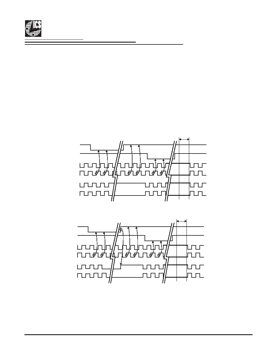
Asserting SRC_STOP# causes all DIF outputs to stop after their next transition (if the control register settings allow the output
to stop). When the SRC_STOP# drive bit is ‘0’, the final state of all stopped DIF outputs is DIF = High and DIF# = Low. There
is no change in output drive current. DIF is driven with 6xIREF. DIF# is not driven, but pulled low by the termination. When the
SRC_STOP# drive bit is ‘1’, the final state of all DIF output pins is Low. Both DIF and DIF# are not driven.
SRC_STOP# - Assertion
All stopped differential outputs resume normal operation in a glitch-free manner. The de-assertion latency to active outputs is
2-6 DIF clock periods, with all DIF outputs resuming simultaneously. If the SRC_STOP# drive control bit is ‘1’ (tri-state), all
stopped DIF outputs must be driven High (>200 mV) within 10 ns of de-assertion.
SRC_STOP# - De-assertion (transition from '0' to '1')
The SRC_STOP# signal is an active-low asynchronous input that cleanly stops and starts the DIF outputs. A valid clock must
be present on SRC_IN for this input to work properly. The SRC_STOP# signal is de-bounced and must remain stable for two
consecutive rising edges of DIF# to be recognized as a valid assertion or de-assertion.
SRC_STOP#
PWRDWN#
SRC_Stop#
DIF (Free Running)
DIF# (Free Running)
DIF (Stoppable)
DIF# (Stoppable)
1mS
PWRDWN#
SRC_Stop#
DIF (Free Running)
DIF# (Free Running)
DIF (Stoppable)
DIF# (Stoppable)
1mS
SRC_STOP_1 (SRC_Stop = Driven, PD = Driven)
SRC_STOP_2 (SRC_Stop =Tristate, PD = Driven)
相关PDF资料 |
PDF描述 |
|---|---|
| 9DB801CGLF | 9DB SERIES, PLL BASED CLOCK DRIVER, 8 TRUE OUTPUT(S), 0 INVERTED OUTPUT(S), PDSO48 |
| 9DB801CFLF | 9DB SERIES, PLL BASED CLOCK DRIVER, 8 TRUE OUTPUT(S), 0 INVERTED OUTPUT(S), PDSO48 |
| 9DB801BFLF | 9DB SERIES, PLL BASED CLOCK DRIVER, 8 TRUE OUTPUT(S), 0 INVERTED OUTPUT(S), PDSO48 |
| 9DB801BGLFT | 9DB SERIES, PLL BASED CLOCK DRIVER, 8 TRUE OUTPUT(S), 0 INVERTED OUTPUT(S), PDSO48 |
| 9DB801CFLFT | 9DB SERIES, PLL BASED CLOCK DRIVER, 8 TRUE OUTPUT(S), 0 INVERTED OUTPUT(S), PDSO48 |
相关代理商/技术参数 |
参数描述 |
|---|---|
| 9DB801BGLFT | 功能描述:时钟缓冲器 8 OUTPUT PCIE GEN1 BUFFER RoHS:否 制造商:Texas Instruments 输出端数量:5 最大输入频率:40 MHz 传播延迟(最大值): 电源电压-最大:3.45 V 电源电压-最小:2.375 V 最大功率耗散: 最大工作温度:+ 85 C 最小工作温度:- 40 C 封装 / 箱体:LLP-24 封装:Reel |
| 9DB801CFLF | 功能描述:时钟缓冲器 8 OUTPUT PCIE GEN1 BUFFER RoHS:否 制造商:Texas Instruments 输出端数量:5 最大输入频率:40 MHz 传播延迟(最大值): 电源电压-最大:3.45 V 电源电压-最小:2.375 V 最大功率耗散: 最大工作温度:+ 85 C 最小工作温度:- 40 C 封装 / 箱体:LLP-24 封装:Reel |
| 9DB801CFLFT | 制造商:Integrated Device Technology Inc 功能描述:PLL Clock Buffer Single 50MHz to 200MHz 48-Pin SSOP T/R 制造商:Integrated Device Technology Inc 功能描述:9DB801CFLFT - Tape and Reel |
| 9DB801CGLF | 功能描述:时钟缓冲器 8 OUTPUT PCIE GEN1 BUFFER RoHS:否 制造商:Texas Instruments 输出端数量:5 最大输入频率:40 MHz 传播延迟(最大值): 电源电压-最大:3.45 V 电源电压-最小:2.375 V 最大功率耗散: 最大工作温度:+ 85 C 最小工作温度:- 40 C 封装 / 箱体:LLP-24 封装:Reel |
| 9DB801CGLFT | 功能描述:时钟缓冲器 8 OUTPUT PCIE GEN1 BUFFER RoHS:否 制造商:Texas Instruments 输出端数量:5 最大输入频率:40 MHz 传播延迟(最大值): 电源电压-最大:3.45 V 电源电压-最小:2.375 V 最大功率耗散: 最大工作温度:+ 85 C 最小工作温度:- 40 C 封装 / 箱体:LLP-24 封装:Reel |
发布紧急采购,3分钟左右您将得到回复。