- 您现在的位置:买卖IC网 > PDF目录25565 > 9DB801CFLFT (INTEGRATED DEVICE TECHNOLOGY INC) 9DB SERIES, PLL BASED CLOCK DRIVER, 8 TRUE OUTPUT(S), 0 INVERTED OUTPUT(S), PDSO48 PDF资料下载
参数资料
| 型号: | 9DB801CFLFT |
| 厂商: | INTEGRATED DEVICE TECHNOLOGY INC |
| 元件分类: | 时钟及定时 |
| 英文描述: | 9DB SERIES, PLL BASED CLOCK DRIVER, 8 TRUE OUTPUT(S), 0 INVERTED OUTPUT(S), PDSO48 |
| 封装: | ROHS COMPLIANT, MO-118, SSOP-48 |
| 文件页数: | 1/19页 |
| 文件大小: | 129K |
| 代理商: | 9DB801CFLFT |
ICS9DB801C
IDTTM/ICSTM Eight Output Differential Buffer for PCI Express (50-200MHz)
9DB801C
REV E 01/27/11
Eight Output Differential Buffer for PCI Express (50-200MHz)
DATASHEET
1
STOP
LOGIC
SRC_IN
SRC_IN#
DIF(7:0))
CONTROL
LOGIC
BYPASS#/PLL
SDATA
SCLK
PD#
SPREAD
COMPATIBLE
PLL
8
IREF
OE_(7:0)
8
LOCK
SRC_STOP#
HIGH_BW#
M
U
X
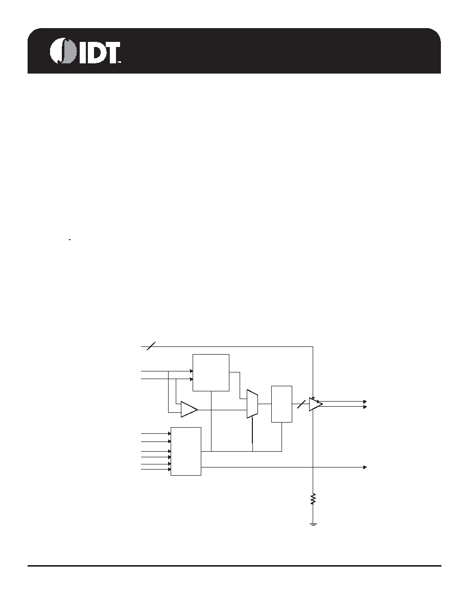
Description
Output Features
The 9DB801C is a DB800 Version 2.0 Yellow Cover part with
PCI Express support. It can be used in PC or embedded
systems to provide outputs that have low cycle-to-cycle jitter
(50ps), low output-to-output skew (100ps), and are PCI Express
gen 1 compliant. The 9DB801C supports a 1 to 8 output
configuration, taking a spread or non spread differential HCSL
input from a CK410(B) main clock such as 954101 and
932S401, or any other differential HCSL pair. 9DB801C can
generate HCSL or LVDS outputs from 50 to 200MHz in PLL
mode or 0 to 400Mhz in bypass mode. There are two de-jittering
modes available selectable through the HIGH_BW# input pin,
high bandwidth mode provides de-jittering for spread inputs and
low bandwidth mode provides extra de-jittering for non-spread
inputs. The SRC_STOP#, PD#, and individual OE# real-time
input pins provide completely programmable power
management control.
8 - 0.7V current-mode differential output pairs
Supports zero delay buffer mode and fanout mode
Bandwidth programming available
Funtional Block Diagram
Key Specifications
Outputs cycle-cycle jitter < 50ps
Outputs skew: 50ps
50 - 200MHz operation
Extended frequency range in bypass mode to 400 MHz
PCI Express Gen I compliant
Real time PLL lock detect output pin
48-pin SSOP/TSSOP package
Available in RoHS compliant packaging
Features/Benefits
Spread spectrum modulation tolerant, 0 to -0.5% down
spread and +/- 0.25% center spread.
Supports undriven differential outputs in PD# and
SRC_STOP# modes for power management.
Supports polarity inversion to the output enables,
SRC_STOP and PD.
Note: Polarities shown for OE_INV = 0.
相关PDF资料 |
PDF描述 |
|---|---|
| 9DB801CGLFT | 9DB SERIES, PLL BASED CLOCK DRIVER, 8 TRUE OUTPUT(S), 0 INVERTED OUTPUT(S), PDSO48 |
| 9DB803DFILFT | 9DB SERIES, PLL BASED CLOCK DRIVER, 8 TRUE OUTPUT(S), 0 INVERTED OUTPUT(S), PDSO48 |
| 9DB803DGILFT | 9DB SERIES, PLL BASED CLOCK DRIVER, 8 TRUE OUTPUT(S), 0 INVERTED OUTPUT(S), PDSO48 |
| 9DB803DFLF | 9DB SERIES, PLL BASED CLOCK DRIVER, 8 TRUE OUTPUT(S), 0 INVERTED OUTPUT(S), PDSO48 |
| 9DB803DFILF | 9DB SERIES, PLL BASED CLOCK DRIVER, 8 TRUE OUTPUT(S), 0 INVERTED OUTPUT(S), PDSO48 |
相关代理商/技术参数 |
参数描述 |
|---|---|
| 9DB801CGLF | 功能描述:时钟缓冲器 8 OUTPUT PCIE GEN1 BUFFER RoHS:否 制造商:Texas Instruments 输出端数量:5 最大输入频率:40 MHz 传播延迟(最大值): 电源电压-最大:3.45 V 电源电压-最小:2.375 V 最大功率耗散: 最大工作温度:+ 85 C 最小工作温度:- 40 C 封装 / 箱体:LLP-24 封装:Reel |
| 9DB801CGLFT | 功能描述:时钟缓冲器 8 OUTPUT PCIE GEN1 BUFFER RoHS:否 制造商:Texas Instruments 输出端数量:5 最大输入频率:40 MHz 传播延迟(最大值): 电源电压-最大:3.45 V 电源电压-最小:2.375 V 最大功率耗散: 最大工作温度:+ 85 C 最小工作温度:- 40 C 封装 / 箱体:LLP-24 封装:Reel |
| 9DB803DFILF | 功能描述:时钟缓冲器 RoHS:否 制造商:Texas Instruments 输出端数量:5 最大输入频率:40 MHz 传播延迟(最大值): 电源电压-最大:3.45 V 电源电压-最小:2.375 V 最大功率耗散: 最大工作温度:+ 85 C 最小工作温度:- 40 C 封装 / 箱体:LLP-24 封装:Reel |
| 9DB803DFILFT | 功能描述:时钟缓冲器 RoHS:否 制造商:Texas Instruments 输出端数量:5 最大输入频率:40 MHz 传播延迟(最大值): 电源电压-最大:3.45 V 电源电压-最小:2.375 V 最大功率耗散: 最大工作温度:+ 85 C 最小工作温度:- 40 C 封装 / 箱体:LLP-24 封装:Reel |
| 9DB803DFLF | 功能描述:时钟缓冲器 8 OUTPUT PCIE GEN2 BUFFER RoHS:否 制造商:Texas Instruments 输出端数量:5 最大输入频率:40 MHz 传播延迟(最大值): 电源电压-最大:3.45 V 电源电压-最小:2.375 V 最大功率耗散: 最大工作温度:+ 85 C 最小工作温度:- 40 C 封装 / 箱体:LLP-24 封装:Reel |
发布紧急采购,3分钟左右您将得到回复。