- 您现在的位置:买卖IC网 > PDF目录25565 > 9DB801CFLFT (INTEGRATED DEVICE TECHNOLOGY INC) 9DB SERIES, PLL BASED CLOCK DRIVER, 8 TRUE OUTPUT(S), 0 INVERTED OUTPUT(S), PDSO48 PDF资料下载
参数资料
| 型号: | 9DB801CFLFT |
| 厂商: | INTEGRATED DEVICE TECHNOLOGY INC |
| 元件分类: | 时钟及定时 |
| 英文描述: | 9DB SERIES, PLL BASED CLOCK DRIVER, 8 TRUE OUTPUT(S), 0 INVERTED OUTPUT(S), PDSO48 |
| 封装: | ROHS COMPLIANT, MO-118, SSOP-48 |
| 文件页数: | 18/19页 |
| 文件大小: | 129K |
| 代理商: | 9DB801CFLFT |
IDTTM/ICSTM Eight Output Differential Buffer for PCI Express (50-200MHz)
9DB801C
REV E 01/27/11
ICS9DB801C
Eight Output Differential Buffer for PCI Express (50-200MHz)
8
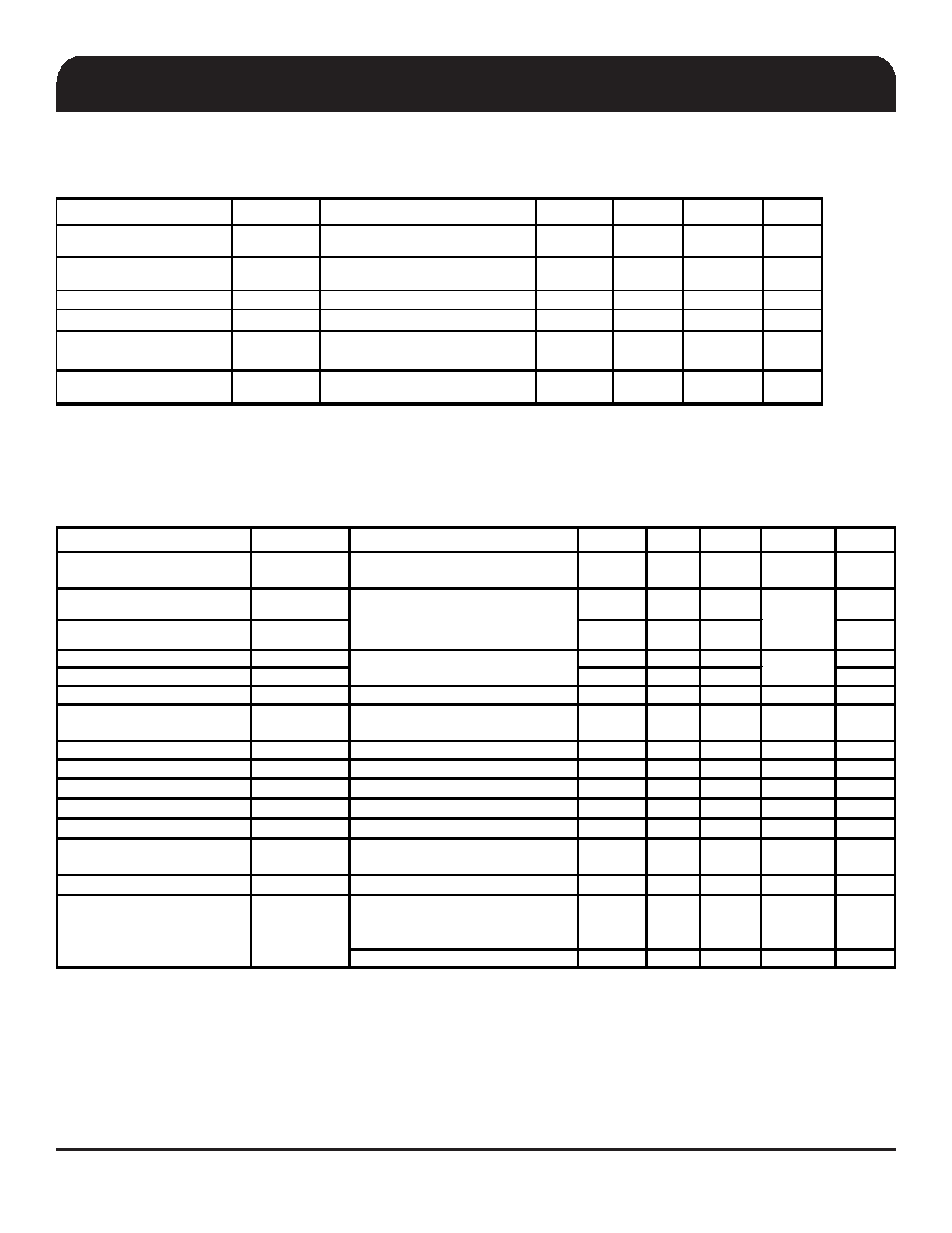
Electrical Characteristics - DIF 0.7V Current Mode Differential Pair
TA = 0 - 70°C; VDD = 3.3 V +/-5%; CL =2pF, RS=33.2
Ω, R
P=49.9
Ω, Ι
REF
= 475Ω
PARAMETER
SYMBOL
CONDITIONS
MIN
TYP
MAX
UNITS
NOTES
Current Source Output
Impedance
Zo
1
VO = Vx
3000
Ω
1
Voltage High
VHigh
660
850
1,3
Voltage Low
VLow
-150
150
1,3
Max Voltage
Vovs
1150
1
Min Voltage
Vuds
-300
1
Crossing Voltage (abs)
Vcross(abs)
250
550
mV
1
Crossing Voltage (var)
d-Vcross
Variation of crossing over all
edges
140
mV
1
Long Accuracy
ppm
see Tperiod min-max values
0
ppm1,2
Rise Time
tr
VOL = 0.175V, VOH = 0.525V
175
700
ps
1
Fall Time
tf
VOH = 0.525V VOL = 0.175V
175
700
ps
1
Rise Time Variation
d-tr
125
ps
1
Fall Time Variation
d-tf
125
ps
1
Duty Cycle
dt3
Measurement from differential
wavefrom
45
55
%
1
Skew
tsk3
VT = 50%
50
ps
1
PLL mode,
Measurement from differential
wavefrom
50
ps
1
BYPASS mode as additive jitter
50
ps1
1Guaranteed by design and characterization, not 100% tested in production.
3I
REF = VDD/(3xRR). For RR = 475
Ω (1%), IREF = 2.32mA. IOH = 6 x IREF and VOH = 0.7V @ ZO=50Ω.
Statistical measurement on single
ended signal using oscilloscope
math function.
mV
Measurement on single ended
signal using absolute value.
mV
2 All Long Term Accuracy and Clock Period specifications are guaranteed with the assumption that the input clock
complies with CK409/CK410 accuracy requirements
Jitter, Cycle to cycle
tjcyc-cyc
Electrical Characteristics - Clock Input Parameters
TA = 0 - 70°C; Supply Voltage VDD = 3.3 V +/-5%
PARAMETER
SYMBOL
CONDITIONS
MIN
MAX
UNITS
NOTES
Differential Input High Voltage
V
IHDIF
Differential inputs
(single-ended measurement)
600
1150
mV
1
Differential Input Low Voltage
V
ILDIF
Differential inputs
(single-ended measurement)
V
SS - 300
300
mV
1
Input Slew Rate - DIF_IN
dv/dt
Measured differentially
0.4
8
V/ns
2
Input Leakage Current
I
IN
V
IN = VDD , VIN = GND
-5
5
uA
1
Input Duty Cycle
dtin
Measurement from differential
wavefrom
45
55
%
1
Input SRC Jitter - Cycle to
Cycle
SRCJ
C2CIn
Differential Measurement
125
ps
1
1 Guaranteed by design and characterization, not 100% tested in production.
2Slew rate measured through Vswing centered around differential zero
相关PDF资料 |
PDF描述 |
|---|---|
| 9DB801CGLFT | 9DB SERIES, PLL BASED CLOCK DRIVER, 8 TRUE OUTPUT(S), 0 INVERTED OUTPUT(S), PDSO48 |
| 9DB803DFILFT | 9DB SERIES, PLL BASED CLOCK DRIVER, 8 TRUE OUTPUT(S), 0 INVERTED OUTPUT(S), PDSO48 |
| 9DB803DGILFT | 9DB SERIES, PLL BASED CLOCK DRIVER, 8 TRUE OUTPUT(S), 0 INVERTED OUTPUT(S), PDSO48 |
| 9DB803DFLF | 9DB SERIES, PLL BASED CLOCK DRIVER, 8 TRUE OUTPUT(S), 0 INVERTED OUTPUT(S), PDSO48 |
| 9DB803DFILF | 9DB SERIES, PLL BASED CLOCK DRIVER, 8 TRUE OUTPUT(S), 0 INVERTED OUTPUT(S), PDSO48 |
相关代理商/技术参数 |
参数描述 |
|---|---|
| 9DB801CGLF | 功能描述:时钟缓冲器 8 OUTPUT PCIE GEN1 BUFFER RoHS:否 制造商:Texas Instruments 输出端数量:5 最大输入频率:40 MHz 传播延迟(最大值): 电源电压-最大:3.45 V 电源电压-最小:2.375 V 最大功率耗散: 最大工作温度:+ 85 C 最小工作温度:- 40 C 封装 / 箱体:LLP-24 封装:Reel |
| 9DB801CGLFT | 功能描述:时钟缓冲器 8 OUTPUT PCIE GEN1 BUFFER RoHS:否 制造商:Texas Instruments 输出端数量:5 最大输入频率:40 MHz 传播延迟(最大值): 电源电压-最大:3.45 V 电源电压-最小:2.375 V 最大功率耗散: 最大工作温度:+ 85 C 最小工作温度:- 40 C 封装 / 箱体:LLP-24 封装:Reel |
| 9DB803DFILF | 功能描述:时钟缓冲器 RoHS:否 制造商:Texas Instruments 输出端数量:5 最大输入频率:40 MHz 传播延迟(最大值): 电源电压-最大:3.45 V 电源电压-最小:2.375 V 最大功率耗散: 最大工作温度:+ 85 C 最小工作温度:- 40 C 封装 / 箱体:LLP-24 封装:Reel |
| 9DB803DFILFT | 功能描述:时钟缓冲器 RoHS:否 制造商:Texas Instruments 输出端数量:5 最大输入频率:40 MHz 传播延迟(最大值): 电源电压-最大:3.45 V 电源电压-最小:2.375 V 最大功率耗散: 最大工作温度:+ 85 C 最小工作温度:- 40 C 封装 / 箱体:LLP-24 封装:Reel |
| 9DB803DFLF | 功能描述:时钟缓冲器 8 OUTPUT PCIE GEN2 BUFFER RoHS:否 制造商:Texas Instruments 输出端数量:5 最大输入频率:40 MHz 传播延迟(最大值): 电源电压-最大:3.45 V 电源电压-最小:2.375 V 最大功率耗散: 最大工作温度:+ 85 C 最小工作温度:- 40 C 封装 / 箱体:LLP-24 封装:Reel |
发布紧急采购,3分钟左右您将得到回复。