- 您现在的位置:买卖IC网 > PDF目录25565 > 9EX21801AKLFT (INTEGRATED DEVICE TECHNOLOGY INC) PLL BASED CLOCK DRIVER, PQCC72 PDF资料下载
参数资料
| 型号: | 9EX21801AKLFT |
| 厂商: | INTEGRATED DEVICE TECHNOLOGY INC |
| 元件分类: | 时钟及定时 |
| 英文描述: | PLL BASED CLOCK DRIVER, PQCC72 |
| 封装: | ROHS COMPLIANT, PLASTIC, MLF-72 |
| 文件页数: | 9/14页 |
| 文件大小: | 160K |
| 代理商: | 9EX21801AKLFT |
IDTTM
18 Output PCIe G2/QPI Differential Buffer with 2:1 input mux
1463B — 01/20/10
ICS9EX21801A
18 Output PCIe G2/QPI Differential Buffer with 2:1 input mux
4
Datasheet
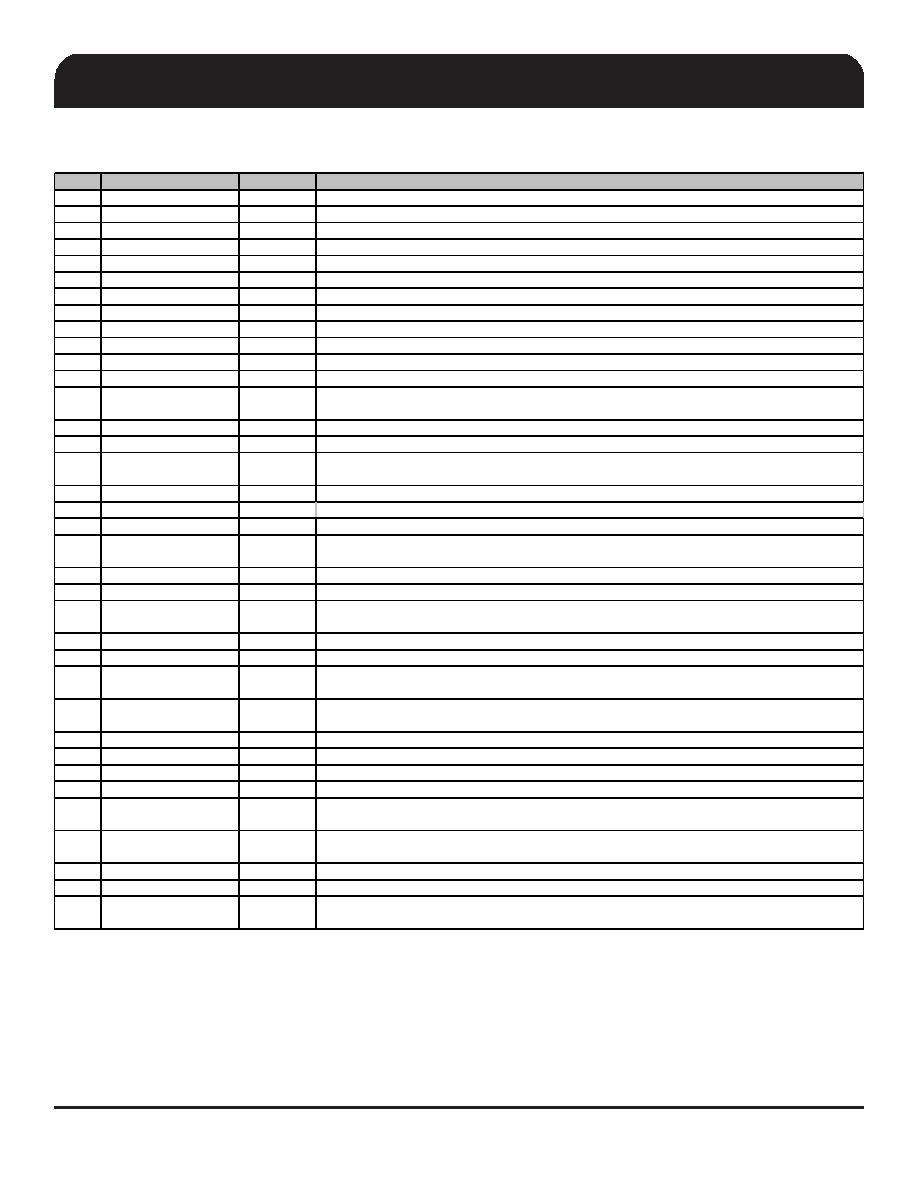
Pin Description (continued)
PIN #
PIN NAME
PIN TYPE
DESCRIPTION
37
DIF_0
OUT
0.7V differential true clock output
38
DIF_0#
OUT
0.7V differential complement clock output
39
DIF_1
OUT
0.7V differential true clock output
40
DIF_1#
OUT
0.7V differential complement clock output
41
DIF_2
OUT
0.7V differential true clock output
42
DIF_2#
OUT
0.7V differential complement clock output
43
VDD
PWR
Power supply, nominal 3.3V
44
GND
PWR
Ground pin.
45
DIF_3
OUT
0.7V differential true clock output
46
DIF_3#
OUT
0.7V differential complement clock output
47
DIF_4
OUT
0.7V differential true clock output
48
DIF_4#
OUT
0.7V differential complement clock output
49
OE5#
IN
Active low input for enabling DIF pair 5.
1 = tri-state outputs, 0 = enable outputs
50
DIF_5
OUT
0.7V differential true clock output
51
DIF_5#
OUT
0.7V differential complement clock output
52
OE6#
IN
Active low input for enabling DIF pair 6.
1 = tri-state outputs, 0 = enable outputs
53
DIF_6
OUT
0.7V differential true clock output
54
DIF_6#
OUT
0.7V differential complement clock output
55
VDD
PWR
Power supply, nominal 3.3V
56
OE7#
IN
Active low input for enabling DIF pair 7.
1 = tri-state outputs, 0 = enable outputs
57
DIF_7
OUT
0.7V differential true clock output
58
DIF_7#
OUT
0.7V differential complement clock output
59
OE8#
IN
Active low input for enabling DIF pair 8.
1 = tri-state outputs, 0 = enable outputs
60
DIF_8
OUT
0.7V differential true clock output
61
DIF_8#
OUT
0.7V differential complement clock output
62
100M_133M#
IN
Input to select operating frequency
0 = 133MHz (QPI), 1 = 100.00MHz (PCIe Gen2)
63
HIBW_BYPM_LOBW#
IN
Trilevel input to select High BW, Bypass Mode or Low BW.
0 = Low BW Mode, Mid= Bypass Mode, 1 = High Bandwidth
64
SMBCLK
IN
Clock pin of SMBUS circuitry, 5V tolerant
65
SMBDAT
I/O
Data pin of SMBUS circuitry, 5V tolerant
66
SMB_A1
IN
SMBus address bit 1
67
SMB_A0
IN
SMBus address bit 0 (LSB)
68
SEL_A_B#
IN
Input to select differential input clock A or differential input clock B.
0 = Input B selected, 1 = Input A selected.
69
CKPWRGD/PD#
IN
Notifies the clock to sample latched inputs on the rising edge, and to power down on the falling
edge.
70
DIF_9
OUT
0.7V differential true clock output
71
DIF_9#
OUT
0.7V differential complement clock output
72
OE9#
IN
Active low input for enabling DIF pair 9.
1 = tri-state outputs, 0 = enable outputs
相关PDF资料 |
PDF描述 |
|---|---|
| 9EX21831AKLFT | 21831 SERIES, PLL BASED CLOCK DRIVER, 18 TRUE OUTPUT(S), 0 INVERTED OUTPUT(S), PQCC72 |
| 9EX21831AKLF | 21831 SERIES, PLL BASED CLOCK DRIVER, 18 TRUE OUTPUT(S), 0 INVERTED OUTPUT(S), PQCC72 |
| 9FG104DGLFT | 400 MHz, PROC SPECIFIC CLOCK GENERATOR, PDSO28 |
| 9FG104DFLF | 400 MHz, PROC SPECIFIC CLOCK GENERATOR, PDSO28 |
| 9FG104DGILF | 400 MHz, PROC SPECIFIC CLOCK GENERATOR, PDSO28 |
相关代理商/技术参数 |
参数描述 |
|---|---|
| 9EX21831AKLF | 功能描述:时钟发生器及支持产品 RoHS:否 制造商:Silicon Labs 类型:Clock Generators 最大输入频率:14.318 MHz 最大输出频率:166 MHz 输出端数量:16 占空比 - 最大:55 % 工作电源电压:3.3 V 工作电源电流:1 mA 最大工作温度:+ 85 C 安装风格:SMD/SMT 封装 / 箱体:QFN-56 |
| 9EX21831AKLFT | 功能描述:时钟发生器及支持产品 RoHS:否 制造商:Silicon Labs 类型:Clock Generators 最大输入频率:14.318 MHz 最大输出频率:166 MHz 输出端数量:16 占空比 - 最大:55 % 工作电源电压:3.3 V 工作电源电流:1 mA 最大工作温度:+ 85 C 安装风格:SMD/SMT 封装 / 箱体:QFN-56 |
| 9EZCA0100000000 | 制造商:Eaton Corporation 功能描述:9E 20 & 30 kVA IAC - Tie for 1+1 Redundant with Maintenance Bypass |
| 9F-110 | 制造商:NA 功能描述: |
| 9F33U0 | 制造商:Thomas & Betts 功能描述:30A,PLG,REV,3P3W,DG,U0,600VAC, |
发布紧急采购,3分钟左右您将得到回复。