- 您现在的位置:买卖IC网 > PDF目录122717 > 9LRS3187BKLF (INTEGRATED DEVICE TECHNOLOGY INC) 133.33 MHz, PROC SPECIFIC CLOCK GENERATOR, PQCC32 PDF资料下载
参数资料
| 型号: | 9LRS3187BKLF |
| 厂商: | INTEGRATED DEVICE TECHNOLOGY INC |
| 元件分类: | 时钟产生/分配 |
| 英文描述: | 133.33 MHz, PROC SPECIFIC CLOCK GENERATOR, PQCC32 |
| 封装: | ROHS COMPLIANT, PLASTIC, MLF-32 |
| 文件页数: | 5/20页 |
| 文件大小: | 193K |
| 代理商: | 9LRS3187BKLF |
IDT Programmable Timing Control Hub for Intel Based Systems
1602E—04/29/11
ICS9LRS3187B
Programmable Timing Control Hub for Intel Based Systems
13
Datasheet
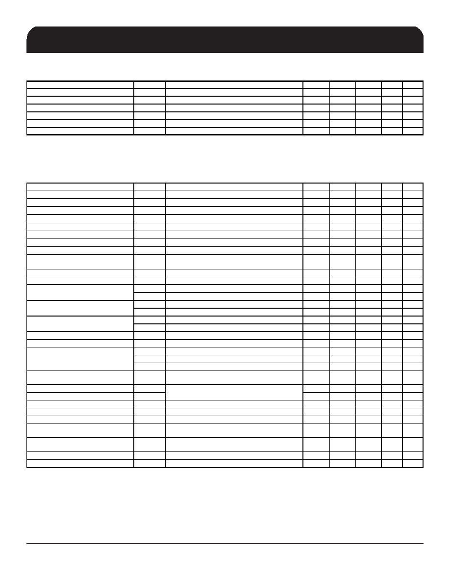
Absolute Maximum Ratings - DC Parameters, Industrial Temperature Range
PARAMETER
SYMBOL
CONDITIONS
MIN
TYP
MAX
UNITS
Notes
Maximum Supply Voltage
VDDxxx
Supply Voltage
4.6
V
1
Maximum Supply Voltage
VDDxxx_IO
Low-Voltage Differential I/O Supply
3.8
V
1
Maximum Input Voltage
VIH
3.3V Tolerant Inputs
4.6
V
1,2
Minimum Input Voltage
VIL
Any Input
GND - 0.5
V
1
Storage Temperature
Ts
-
-65
150
°C
1
Input ESD protection
ESD prot
Human Body Model
2000
V
1,3
1 Operation under these conditions is neither implied, nor guaranteed.
Notes: (unless otherwise noted, guaranteed by design and characterization, not 100% tested in production).
2 Maximum VIH is not to exceed VDD
3 Human Body Model
Electrical Characteristics - Input/Supply/Common Output DC Parameters, Industrial Temperature Range
PARAMETER
SYMBOL
CONDITIONS
MIN
TYP
MAX
UNITS
Notes
Ambient Operating Temp
Tambind
Industrial Range
-40
85
°C
Supply Voltage, Core
VDDxxx
Supply Voltage
3.135
3.3
3.465
V
Supply Voltage, I/O
VDDxxx_IO
Low-Voltage Differential I/O Supply
0.9975
1.05
3.465
V
5
Input High Voltage
VIHSE
Single-ended 3.3V inputs
2
2.4
VDD + 0.3
V
3
Input Low Voltage
VILSE
Single-ended 3.3V inputs
VSS - 0.3
0.4
0.8
V
3
Low Threshold Input - High Voltage
VIH_FSC
3.3 V +/-5%, Voltage for which FSC = '1'
0.7
3.3
V
4
Low Threshold Input - Low Voltage
VIL_FSC
3.3 V +/-5%
VSS - 0.3
0.35
V
Input Leakage Current
IIN
VIN = VDD , VIN = GND
-5
5
uA
2
Input Leakage Current
IINRES
Inputs with pull up or pull down resistors
VIN = VDD , VIN = GND
-200
200
uA
Output High Voltage
VOHSE
Single-ended outputs, IOH = -1mA
2.4
V
1
Output Low Voltage
VOLSE
Single-ended outputs, IOL = 1 mA
0.4
V
1
IDDOP3.3
Full Active, CL = Full load; Idd 3.3V
92
110
mA
IDDOPIO
Full Active, CL = Full load; IDD IO
18
25
mA
5
IDDiAMT3.3
M1 mode, 3.3V Rail
48
65
mA
IDDiAMTIO
M1 Mode, IO Rail
6
15
mA
5
IDDPD3.3
Power down mode, 3.3V Rail
3.2
8
mA
IDDPDIO
Power down mode, IO Rail
0
0.05
mA
5
Input Frequency
Fi
VDD = 3.3 V
14.318
15
MHz
Pin Inductance
Lpin
57
nH
CIN
Logic Inputs
1.5
4
5
pF
COUT
Output pin capacitance
5
6
pF
CINX
X1 & X2 pins
4
6
pF
Clk Stabilization
TSTAB
From VDD Power-Up or de-assertion of PD to 1st clock
1.8
ms
Tfall_SE
TFALL
10
ns
1
Trise_SE
TRISE
10
ns
1
SMBus Voltage
VDD
2.7
3.3
5.5
V
Low-level Output Voltage
VOLSMB
@ IPULLUP
0.4
V
Current sinking at VOLSMB = 0.4 V
IPULLUP
SMB Data Pin
4
5
mA
SCLK/SDATA
Clock/Data Rise Time
TRI2C
(Max VIL - 0.15) to
(Min VIH + 0.15)
1000
ns
SCLK/SDATA
Clock/Data Fall Time
TFI2C
(Min VIH + 0.15) to
(Max VIL - 0.15)
300
ns
Maximum SMBus Operating Frequency
FSMBUS
100
kHz
Spread Spectrum Modulation Frequency
fSSMOD
Triangular Modulation
30
32.54
33
kHz
1Signal is required to be monotonic in this region.
2 Input leakage current does not include inputs with pull-up or pull-down resistors
4 Frequency Select pins which have tri-level input
5 If present, not all parts have this feature.
Powerdown Current
Input Capacitance
Fall/rise time of all 3.3V control inputs from 20-80%
Operating Supply Current
iAMT Mode Current
Notes: (unless otherwise noted, guaranteed by design and characterization, not 100% tested in production).
3 3.3V referenced inputs are: SCLK, SDATA, and CKPWRGD
相关PDF资料 |
PDF描述 |
|---|---|
| 935262233118 | 16 I/O, PIA-GENERAL PURPOSE, PDSO24 |
| 935262403118 | 0 TIMER(S), REAL TIME CLOCK, PDSO8 |
| 935261475512 | 8 CHANNEL(S), 500K bps, SERIAL COMM CONTROLLER, PQCC84 |
| 9LPRS365BKLF | SPECIALTY MICROPROCESSOR CIRCUIT, PQCC64 |
| 91W-G28AC-6-CG9 | SINGLE COLOR DISPLAY CLUSTER, GREEN, 7.1 mm |
相关代理商/技术参数 |
参数描述 |
|---|---|
| 9LRS3187BKLFT | 功能描述:时钟合成器/抖动清除器 RoHS:否 制造商:Skyworks Solutions, Inc. 输出端数量: 输出电平: 最大输出频率: 输入电平: 最大输入频率:6.1 GHz 电源电压-最大:3.3 V 电源电压-最小:2.7 V 封装 / 箱体:TSSOP-28 封装:Reel |
| 9LRS3197AKLF | 功能描述:时钟发生器及支持产品 RoHS:否 制造商:Silicon Labs 类型:Clock Generators 最大输入频率:14.318 MHz 最大输出频率:166 MHz 输出端数量:16 占空比 - 最大:55 % 工作电源电压:3.3 V 工作电源电流:1 mA 最大工作温度:+ 85 C 安装风格:SMD/SMT 封装 / 箱体:QFN-56 |
| 9LRS3197AKLFT | 功能描述:时钟合成器/抖动清除器 RoHS:否 制造商:Skyworks Solutions, Inc. 输出端数量: 输出电平: 最大输出频率: 输入电平: 最大输入频率:6.1 GHz 电源电压-最大:3.3 V 电源电压-最小:2.7 V 封装 / 箱体:TSSOP-28 封装:Reel |
| 9LRS4103AKLFT | 功能描述:时钟发生器及支持产品 RoHS:否 制造商:Silicon Labs 类型:Clock Generators 最大输入频率:14.318 MHz 最大输出频率:166 MHz 输出端数量:16 占空比 - 最大:55 % 工作电源电压:3.3 V 工作电源电流:1 mA 最大工作温度:+ 85 C 安装风格:SMD/SMT 封装 / 箱体:QFN-56 |
| 9LRS4103BKLF | 功能描述:时钟发生器及支持产品 RoHS:否 制造商:Silicon Labs 类型:Clock Generators 最大输入频率:14.318 MHz 最大输出频率:166 MHz 输出端数量:16 占空比 - 最大:55 % 工作电源电压:3.3 V 工作电源电流:1 mA 最大工作温度:+ 85 C 安装风格:SMD/SMT 封装 / 箱体:QFN-56 |
发布紧急采购,3分钟左右您将得到回复。