- 您现在的位置:买卖IC网 > PDF目录67354 > A1174EEWLT-P MAGNETIC FIELD SENSOR-HALL EFFECT, -5.5-5.5mT, 300mV, RECTANGULAR, SURFACE MOUNT PDF资料下载
参数资料
| 型号: | A1174EEWLT-P |
| 元件分类: | 磁阻传感器 |
| 英文描述: | MAGNETIC FIELD SENSOR-HALL EFFECT, -5.5-5.5mT, 300mV, RECTANGULAR, SURFACE MOUNT |
| 封装: | 1.50 X 2 MM, 0.40 MM HEIGHT, LEAD FREE, DFN-6 |
| 文件页数: | 12/13页 |
| 文件大小: | 316K |
| 代理商: | A1174EEWLT-P |
Ultrasensitive Hall Effect Latch
with Internally or Externally Controlled Sample and Sleep Periods
for Track Ball and Scroll Wheel Applications
A1174
8
Allegro MicroSystems, Inc.
115 Northeast Cutoff
Worcester, Massachusetts 01615-0036 U.S.A.
1.508.853.5000; www.allegromicro.com
Functional Description
Output State Operation
The output state (VOUT pin) of this device switches to low (on)
when an incident magnetic field, perpendicular to the Hall ele-
ment, exceeds the operate point threshold, BOP. After turn-on,
the output voltage is VOUT(SAT) (see figure 2). When the magnetic
field is reduced below the release point, BRP, the device output
goes high (off), VOUT(HIGH). The difference in the magnetic oper-
ate and release points is the hysteresis, BHYS, of the device. This
built-in hysteresis allows clean switching of the output even in
the presence of external mechanical vibration and electrical noise.
Removal of the magnetic field leaves the device output latched
low (on) if the last crossed switchpoint is BOP, or latched high
(off) if the last crossed switchpoint is BRP.
Powering-on the device in the hysteresis range (less than BOP and
higher than BRP) gives an indeterminate output state. The correct
state is attained after the first excursion beyond BOP or BRP .
Micro-power Operation
Micro-power operation of the device involves duty cycle control
achieved by:
powering all circuits in the chip and latching the device output
state at the end of awake state periods, and
turning off the bias current to most circuits in the chip and
maintaining the device output state through sleep state periods.
This is illustrated in figure 3. The awake state duration, tawake_x,
is common in all defined modes of operation. The sleep state
duration is set at a longer duration than the awake period in order
to conserve power. During the sleep state, current consumption
is insignificant (equal to IDD(DIS)), but the device output does not
switch in response to changing incident magnetic fields.
The device shows maximum current consumption, IDD(EN), dur-
ing the awake state and minimal current consumption, IDD(DIS),
during the sleep state. Average current, IDD(AV), for micro-power
operation is derived from following formula:
IDD(AV)
.
IDD(EN) × tawake_x + IDD(DIS) × tsleep_x
=
tperiod_x
Three micro-power control modes are available:
Normal Clock mode
External Clock mode
Dual Clock mode
Selection of clock mode is determined by the configuration of
the EXTERNAL_CLK pin and the DUAL_CLK pin, and applied
voltages as illustrated in figure 4 and table 1.
Normal Clock Mode
When both device clock pins are left
floating or are grounded, the internal timing circuitry activates
the device for tawake_norm and deactivates it for the remainder,
tsleep, of the duty cycle period, tperiod_norm. The short awake time
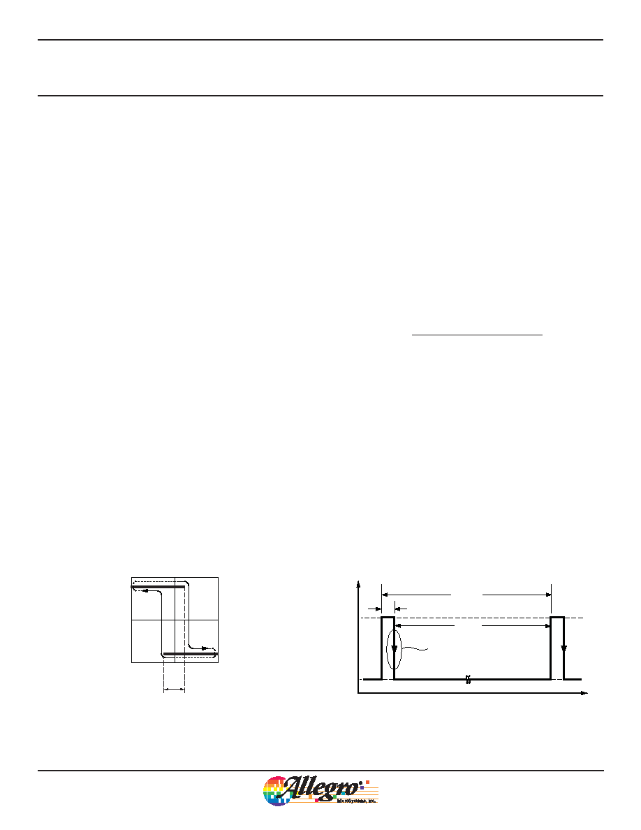
Figure 2. Device output switching logic
B
OP
B
RP
BHYS
VOUT(HIGH) (off)
V
OUT
VOUT(SAT)(on)
Switch
to
Low
Switch
to
High
B+
B–
0
V+
Figure 3. Micro-power behavior of the device
0
t
tperiod_x
tawake_x
tsleep_x
I
DD(EN)
I
DD
IDD(DIS)
Sample and
output latched
相关PDF资料 |
PDF描述 |
|---|---|
| A1174EEWLT-T | MAGNETIC FIELD SENSOR-HALL EFFECT, -5.5-5.5mT, 300mV, RECTANGULAR, SURFACE MOUNT |
| A1193LUA-T | MAGNETIC FIELD SENSOR-HALL EFFECT, 1-20mT, RECTANGULAR, THROUGH HOLE MOUNT |
| A1192LLHLT-T | MAGNETIC FIELD SENSOR-HALL EFFECT, 1-20mT, RECTANGULAR, SURFACE MOUNT |
| A1190LUA-T | MAGNETIC FIELD SENSOR-HALL EFFECT, 1-20mT, RECTANGULAR, THROUGH HOLE MOUNT |
| A1192LUA-T | MAGNETIC FIELD SENSOR-HALL EFFECT, 1-20mT, RECTANGULAR, THROUGH HOLE MOUNT |
相关代理商/技术参数 |
参数描述 |
|---|---|
| A11755-000 | 制造商:TE Connectivity 功能描述:TTMS-6.4-8 - Tape and Reel |
| A1175-HBL | 制造商:未知厂家 制造商全称:未知厂家 功能描述:SPECIFICATION FOR APPROVAL |
| A1175-HBL TC | 制造商:SUNON 功能描述:FAN 172MM 115VAC |
| A1175-HBL TC.GN | 制造商:SUNON 功能描述:FAN 172MM 115VAC 制造商:SUNON 功能描述:FAN, 172MM, 115VAC 制造商:SUNON 功能描述:AXIAL FAN, 172MM, 115VDC,200CFM, 55dBA; Frame Dimensions:171mm x 151mm x 51mm; Supply Voltage:115VAC; Current Rating:480mA; Flow Rate - Imperial:200cu.ft/min; Flow Rate - Metric:6.69m /min; Noise Rating:55dBA; Bearing Type:Ball ;RoHS Compliant: Yes |
| A1175-HBL.T.GN | 制造商:SUNON 功能描述:A1175-HBL.T.GN Fan Size mm: 171x151x51 Bearing: 2 Balls Voltage: 115 |
发布紧急采购,3分钟左右您将得到回复。