参数资料
| 型号: | A1440A-1VQ100C |
| 厂商: | Microsemi SoC |
| 文件页数: | 29/90页 |
| 文件大小: | 0K |
| 描述: | IC FPGA 4K GATES 100-VQFP |
| 产品变化通告: | A1440A Family Discontinuation 24/Jan/2012 |
| 标准包装: | 90 |
| 系列: | ACT™ 3 |
| LAB/CLB数: | 564 |
| 输入/输出数: | 83 |
| 门数: | 4000 |
| 电源电压: | 4.5 V ~ 5.5 V |
| 安装类型: | 表面贴装 |
| 工作温度: | 0°C ~ 70°C |
| 封装/外壳: | 100-TQFP |
| 供应商设备封装: | 100-VQFP(14x14) |
第1页第2页第3页第4页第5页第6页第7页第8页第9页第10页第11页第12页第13页第14页第15页第16页第17页第18页第19页第20页第21页第22页第23页第24页第25页第26页第27页第28页当前第29页第30页第31页第32页第33页第34页第35页第36页第37页第38页第39页第40页第41页第42页第43页第44页第45页第46页第47页第48页第49页第50页第51页第52页第53页第54页第55页第56页第57页第58页第59页第60页第61页第62页第63页第64页第65页第66页第67页第68页第69页第70页第71页第72页第73页第74页第75页第76页第77页第78页第79页第80页第81页第82页第83页第84页第85页第86页第87页第88页第89页第90页
Accelerator Series FPGAs – ACT 3 Family
R e visio n 3
2 - 27
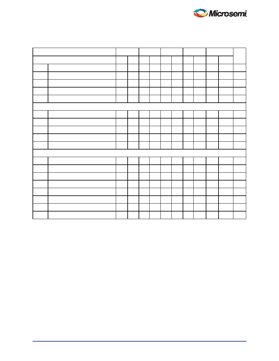
A1425A, A14V25A Timing Characteristics (continued)
Table 2-23 A1425A, A14V25A Worst-Case Commercial Conditions, VCC = 4.75 V, TJ = 70°C
I/O Module Input Propagation Delays
–3 Speed1 –2 Speed1 –1 Speed Std. Speed 3.3 V Speed1 Units
Parameter/Description
Min. Max. Min. Max. Min. Max. Min. Max.
Min.
Max.
tINY
Input Data Pad to Y
2.8
3.2
3.6
4.2
5.5
ns
tICKY
Input Reg IOCLK Pad to Y
4.7
5.3
6.0
7.0
9.2
ns
tOCKY
Output Reg IOCLK Pad to Y
4.7
5.3
6.0
7.0
9.2
ns
tICLRY Input Asynchronous Clear to Y
4.7
5.3
6.0
7.0
9.2
ns
tOCLRY Output Asynchronous Clear to Y
4.7
5.3
6.0
7.0
9.2
ns
Predicted Input Routing Delays2
tRD1
FO = 1 Routing Delay
0.9
1.0
1.1
1.3
1.7
ns
tRD2
FO = 2 Routing Delay
1.2
1.4
1.6
1.8
2.4
ns
tRD3
FO = 3 Routing Delay
1.4
1.6
1.8
2.1
2.8
ns
tRD4
FO = 4 Routing Delay
1.7
1.9
2.2
2.5
3.3
ns
tRD8
FO = 8 Routing Delay
2.8
3.2
3.6
4.2
5.5
ns
I/O Module Sequential Timing (wrt IOCLK pad)
tINH
Input F-F Data Hold
0.0
ns
tINSU
Input F-F Data Setup
1.8
2.0
2.3
2.7
3.0
ns
tIDEH
Input Data Enable Hold
0.0
ns
tIDESU Input Data Enable Setup
5.8
6.5
7.5
8.6
ns
tOUTH
Output F-F Data hold
0.7
0.8
0.9
1.0
ns
tOUTSU Output F-F Data Setup
0.7
0.8
0.9
1.0
ns
tODEH Output Data Enable Hold
0.3
0.4
0.5
ns
fODESU Output Data Enable Setup
1.3
1.5
1.7
2.0
ns
Notes: *
1. The –2 and –3 speed grades have been discontinued. Refer to PDN 0104, PDN 0203, PDN 0604, and PDN 1004 at
2. Routing delays are for typical designs across worst-case operating conditions. These parameters should be used for
estimating device performance. Post-route timing analysis or simulation is required to determine actual worst-case
performance. Post-route timing is based on actual routing delay measurements performed on the device prior to
shipment.
相关PDF资料 |
PDF描述 |
|---|---|
| IDT71V424L15PHG8 | IC SRAM 4MBIT 15NS 44TSOP |
| IDT71V424L12PHG8 | IC SRAM 4MBIT 12NS 44TSOP |
| IDT7164S25YG | IC SRAM 64KBIT 25NS 28SOJ |
| IDT71V632S6PFG | IC SRAM 2MBIT 6NS 100TQFP |
| IDT71V632S7PFG | IC SRAM 2MBIT 7NS 100TQFP |
相关代理商/技术参数 |
参数描述 |
|---|---|
| A1440A-1VQ100I | 功能描述:IC FPGA 4K GATES 100-VQFP RoHS:否 类别:集成电路 (IC) >> 嵌入式 - FPGA(现场可编程门阵列) 系列:ACT™ 3 产品变化通告:XC4000(E,L) Discontinuation 01/April/2002 标准包装:24 系列:XC4000E/X LAB/CLB数:100 逻辑元件/单元数:238 RAM 位总计:3200 输入/输出数:80 门数:3000 电源电压:4.5 V ~ 5.5 V 安装类型:表面贴装 工作温度:-40°C ~ 100°C 封装/外壳:120-BCBGA 供应商设备封装:120-CPGA(34.55x34.55) |
| A1440A-1VQG100C | 功能描述:IC FPGA 4K GATES 100-VQFP RoHS:是 类别:集成电路 (IC) >> 嵌入式 - FPGA(现场可编程门阵列) 系列:ACT™ 3 产品变化通告:XC4000(E,L) Discontinuation 01/April/2002 标准包装:24 系列:XC4000E/X LAB/CLB数:100 逻辑元件/单元数:238 RAM 位总计:3200 输入/输出数:80 门数:3000 电源电压:4.5 V ~ 5.5 V 安装类型:表面贴装 工作温度:-40°C ~ 100°C 封装/外壳:120-BCBGA 供应商设备封装:120-CPGA(34.55x34.55) |
| A1440A-1VQG100I | 功能描述:IC FPGA 4K GATES 100-VQFP RoHS:是 类别:集成电路 (IC) >> 嵌入式 - FPGA(现场可编程门阵列) 系列:ACT™ 3 产品变化通告:XC4000(E,L) Discontinuation 01/April/2002 标准包装:24 系列:XC4000E/X LAB/CLB数:100 逻辑元件/单元数:238 RAM 位总计:3200 输入/输出数:80 门数:3000 电源电压:4.5 V ~ 5.5 V 安装类型:表面贴装 工作温度:-40°C ~ 100°C 封装/外壳:120-BCBGA 供应商设备封装:120-CPGA(34.55x34.55) |
| A1440A-2PG175C | 制造商:未知厂家 制造商全称:未知厂家 功能描述:Field Programmable Gate Array (FPGA) |
| A1440A-2PL84C | 制造商:Microsemi Corporation 功能描述:FPGA ACT 3 4K GATES 564 CELLS 200MHZ 0.8UM 5V 84PLCC - Rail/Tube 制造商:Microsemi SOC Products Group 功能描述:FPGA ACT 3 4K GATES 564 CELLS 200MHZ 0.8UM 5V 84PLCC - Rail/Tube |
发布紧急采购,3分钟左右您将得到回复。