参数资料
| 型号: | A1440A-1VQ100C |
| 厂商: | Microsemi SoC |
| 文件页数: | 3/90页 |
| 文件大小: | 0K |
| 描述: | IC FPGA 4K GATES 100-VQFP |
| 产品变化通告: | A1440A Family Discontinuation 24/Jan/2012 |
| 标准包装: | 90 |
| 系列: | ACT™ 3 |
| LAB/CLB数: | 564 |
| 输入/输出数: | 83 |
| 门数: | 4000 |
| 电源电压: | 4.5 V ~ 5.5 V |
| 安装类型: | 表面贴装 |
| 工作温度: | 0°C ~ 70°C |
| 封装/外壳: | 100-TQFP |
| 供应商设备封装: | 100-VQFP(14x14) |
第1页第2页当前第3页第4页第5页第6页第7页第8页第9页第10页第11页第12页第13页第14页第15页第16页第17页第18页第19页第20页第21页第22页第23页第24页第25页第26页第27页第28页第29页第30页第31页第32页第33页第34页第35页第36页第37页第38页第39页第40页第41页第42页第43页第44页第45页第46页第47页第48页第49页第50页第51页第52页第53页第54页第55页第56页第57页第58页第59页第60页第61页第62页第63页第64页第65页第66页第67页第68页第69页第70页第71页第72页第73页第74页第75页第76页第77页第78页第79页第80页第81页第82页第83页第84页第85页第86页第87页第88页第89页第90页
Accelerator Series FPGAs – ACT 3 Family
R e visio n 3
2 -3
The S-module contains a full implementation of the C-module plus a clearable sequential element that
can either implement a latch or flip-flop function. The S-module can therefore implement any function
implemented by the C-module. This allows complex combinatorial-sequential functions to be
implemented with no delay penalty. The Designer Series Development System will automatically
combine any C-module macro driving an S-module macro into the S-module, thereby freeing up a logic
module and eliminating a module delay.
The clear input CLR is accessible from the routing channel. In addition, the clock input may be connected
to one of three clock networks: CLKA, CLKB, or HCLK. The C-module and S-module functional
descriptions are shown in Figure 2-2 and Figure 2-3 on page 2-2. The clock selection is determined by a
multiplexer select at the clock input to the S-module.
I/Os
I/O Modules
I/O modules provide an interface between the array and the I/O Pad Drivers. I/O modules are located in
the array and access the routing channels in a similar fashion to logic modules. The I/O module
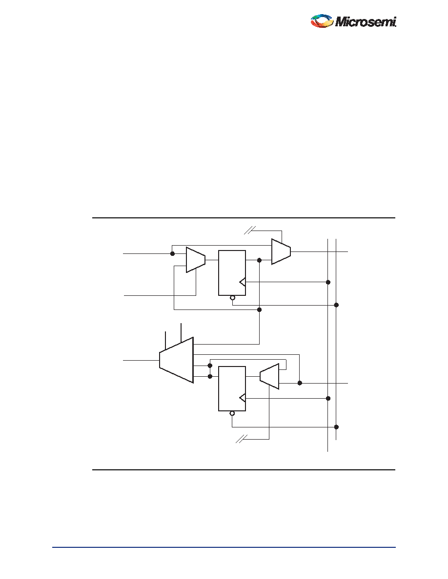
schematic is shown in Figure 4. The signals DataIn and DataOut connect to the I/O pad driver.
Each I/O module contains two D-type flip-flops. Each flip-flop is connected to the dedicated I/O clock
(IOCLK). Each flip-flop can be bypassed by nonsequential I/Os. In addition, each flip-flop contains a data
enable input that can be accessed from the routing channels (ODE and IDE). The asynchronous
preset/clear input is driven by the dedicated preset/clear network (IOPCL). Either preset or clear can be
selected individually on an I/O module by I/O module basis.
Figure 2-4
Functional Diagram for I/O Module
D
DATAOUT
D
Q
CLR/PRE
DATAIN
IOCLK
IOPCL
Y
D
Q
CLR/PRE
ODE
MUX
1
0
MUX
1
0
MUX
0
1
MUX
3
0
1
2
S1
S0
相关PDF资料 |
PDF描述 |
|---|---|
| IDT71V424L15PHG8 | IC SRAM 4MBIT 15NS 44TSOP |
| IDT71V424L12PHG8 | IC SRAM 4MBIT 12NS 44TSOP |
| IDT7164S25YG | IC SRAM 64KBIT 25NS 28SOJ |
| IDT71V632S6PFG | IC SRAM 2MBIT 6NS 100TQFP |
| IDT71V632S7PFG | IC SRAM 2MBIT 7NS 100TQFP |
相关代理商/技术参数 |
参数描述 |
|---|---|
| A1440A-1VQ100I | 功能描述:IC FPGA 4K GATES 100-VQFP RoHS:否 类别:集成电路 (IC) >> 嵌入式 - FPGA(现场可编程门阵列) 系列:ACT™ 3 产品变化通告:XC4000(E,L) Discontinuation 01/April/2002 标准包装:24 系列:XC4000E/X LAB/CLB数:100 逻辑元件/单元数:238 RAM 位总计:3200 输入/输出数:80 门数:3000 电源电压:4.5 V ~ 5.5 V 安装类型:表面贴装 工作温度:-40°C ~ 100°C 封装/外壳:120-BCBGA 供应商设备封装:120-CPGA(34.55x34.55) |
| A1440A-1VQG100C | 功能描述:IC FPGA 4K GATES 100-VQFP RoHS:是 类别:集成电路 (IC) >> 嵌入式 - FPGA(现场可编程门阵列) 系列:ACT™ 3 产品变化通告:XC4000(E,L) Discontinuation 01/April/2002 标准包装:24 系列:XC4000E/X LAB/CLB数:100 逻辑元件/单元数:238 RAM 位总计:3200 输入/输出数:80 门数:3000 电源电压:4.5 V ~ 5.5 V 安装类型:表面贴装 工作温度:-40°C ~ 100°C 封装/外壳:120-BCBGA 供应商设备封装:120-CPGA(34.55x34.55) |
| A1440A-1VQG100I | 功能描述:IC FPGA 4K GATES 100-VQFP RoHS:是 类别:集成电路 (IC) >> 嵌入式 - FPGA(现场可编程门阵列) 系列:ACT™ 3 产品变化通告:XC4000(E,L) Discontinuation 01/April/2002 标准包装:24 系列:XC4000E/X LAB/CLB数:100 逻辑元件/单元数:238 RAM 位总计:3200 输入/输出数:80 门数:3000 电源电压:4.5 V ~ 5.5 V 安装类型:表面贴装 工作温度:-40°C ~ 100°C 封装/外壳:120-BCBGA 供应商设备封装:120-CPGA(34.55x34.55) |
| A1440A-2PG175C | 制造商:未知厂家 制造商全称:未知厂家 功能描述:Field Programmable Gate Array (FPGA) |
| A1440A-2PL84C | 制造商:Microsemi Corporation 功能描述:FPGA ACT 3 4K GATES 564 CELLS 200MHZ 0.8UM 5V 84PLCC - Rail/Tube 制造商:Microsemi SOC Products Group 功能描述:FPGA ACT 3 4K GATES 564 CELLS 200MHZ 0.8UM 5V 84PLCC - Rail/Tube |
发布紧急采购,3分钟左右您将得到回复。