参数资料
| 型号: | A1440A-VQ100I |
| 厂商: | Microsemi SoC |
| 文件页数: | 4/90页 |
| 文件大小: | 0K |
| 描述: | IC FPGA 4K GATES 100-VQFP |
| 产品变化通告: | A1440A Family Discontinuation 24/Jan/2012 |
| 标准包装: | 90 |
| 系列: | ACT™ 3 |
| LAB/CLB数: | 564 |
| 输入/输出数: | 83 |
| 门数: | 4000 |
| 电源电压: | 4.5 V ~ 5.5 V |
| 安装类型: | 表面贴装 |
| 工作温度: | -40°C ~ 85°C |
| 封装/外壳: | 100-TQFP |
| 供应商设备封装: | 100-VQFP(14x14) |
第1页第2页第3页当前第4页第5页第6页第7页第8页第9页第10页第11页第12页第13页第14页第15页第16页第17页第18页第19页第20页第21页第22页第23页第24页第25页第26页第27页第28页第29页第30页第31页第32页第33页第34页第35页第36页第37页第38页第39页第40页第41页第42页第43页第44页第45页第46页第47页第48页第49页第50页第51页第52页第53页第54页第55页第56页第57页第58页第59页第60页第61页第62页第63页第64页第65页第66页第67页第68页第69页第70页第71页第72页第73页第74页第75页第76页第77页第78页第79页第80页第81页第82页第83页第84页第85页第86页第87页第88页第89页第90页
Detailed Specifications
2- 4
R e v ision 3
The I/O module output Y is used to bring Pad signals into the array or to feed the output register back into
the array. This allows the output register to be used in high-speed state machine applications. Side I/O
modules have a dedicated output segment for Y extending into the routing channels above and below
(similar to logic modules). Top/Bottom I/O modules have no dedicated output segment. Signals coming
into the chip from the top or bottom are routed using F-fuses and LVTs (F-fuses and LVTs are explained
in detail in the routing section).
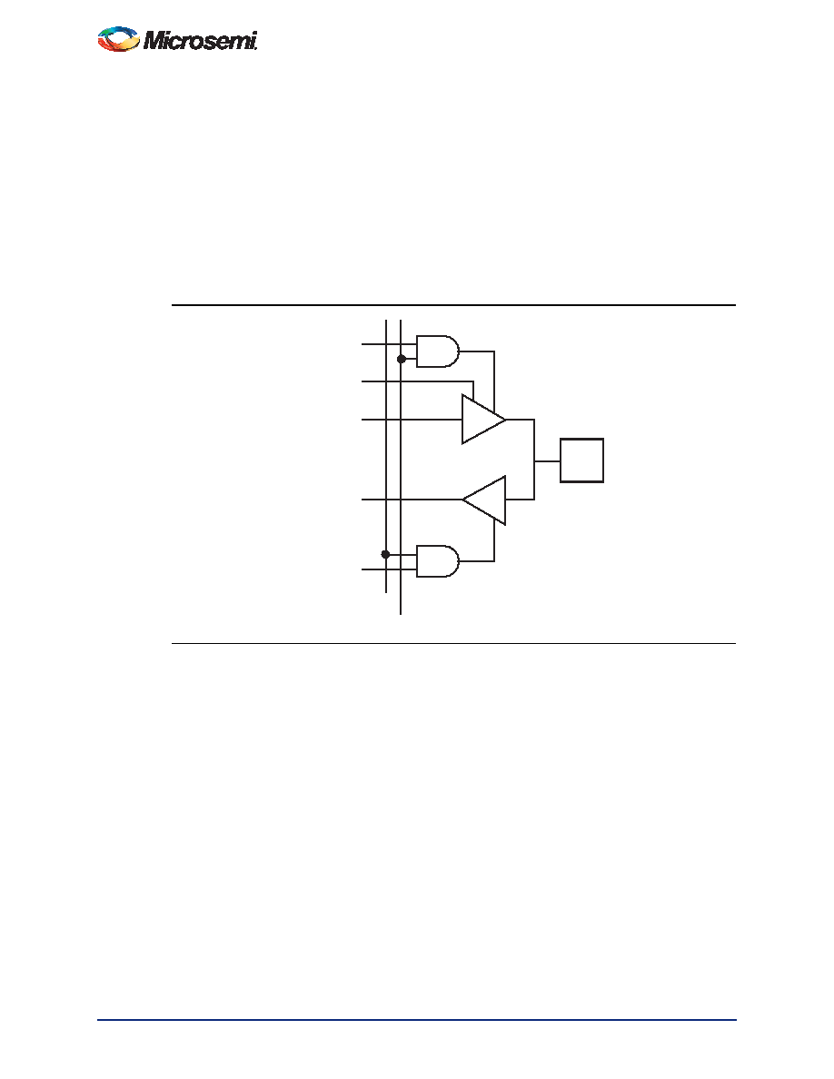
I/O Pad Drivers
All pad drivers are capable of being tristate. Each buffer connects to an associated I/O module with four
signals: OE (Output Enable), IE (Input Enable), DataOut, and DataIn. Certain special signals used only
during programming and test also connect to the pad drivers: OUTEN (global output enable), INEN
(global input enable), and SLEW (individual slew selection). See Figure 2-5.
Special I/Os
The special I/Os are of two types: temporary and permanent. Temporary special I/Os are used during
programming and testing. They function as normal I/Os when the MODE pin is inactive. Permanent
special I/Os are user programmed as either normal I/Os or special I/Os. Their function does not change
once the device has been programmed. The permanent special I/Os consist of the array clock input
buffers (CLKA and CLKB), the hard-wired array clock input buffer (HCLK), the hard-wired I/O clock input
buffer (IOCLK), and the hard-wired I/O register preset/clear input buffer (IOPCL). Their function is
determined by the I/O macros selected.
Clock Networks
The ACT 3 architecture contains four clock networks: two high-performance dedicated clock networks
and two general purpose routed networks. The high-performance networks function up to 200 MHz,
while the general purpose routed networks function up to 150 MHz.
Figure 2-5
Function Diagram for I/O Pad Driver
PAD
OE
SLEW
DATAOUT
DATAIN
IEN
INEN
OUTEN
相关PDF资料 |
PDF描述 |
|---|---|
| A1440A-VQ100C | IC FPGA 4K GATES 100-VQFP |
| A1425A-VQG100I | IC FPGA 2500 GATES 100-VQFP |
| A1425A-VQ100C | IC FPGA 2500 GATES 100-VQFP |
| IDT71V416S12BEG8 | IC SRAM 4MBIT 12NS 48FBGA |
| HMC65DRTS-S734 | CONN EDGECARD 130PS DIP .100 SLD |
相关代理商/技术参数 |
参数描述 |
|---|---|
| A1440A-VQG100C | 功能描述:IC FPGA 4K GATES 100-VQFP RoHS:是 类别:集成电路 (IC) >> 嵌入式 - FPGA(现场可编程门阵列) 系列:ACT™ 3 产品变化通告:XC4000(E,L) Discontinuation 01/April/2002 标准包装:24 系列:XC4000E/X LAB/CLB数:100 逻辑元件/单元数:238 RAM 位总计:3200 输入/输出数:80 门数:3000 电源电压:4.5 V ~ 5.5 V 安装类型:表面贴装 工作温度:-40°C ~ 100°C 封装/外壳:120-BCBGA 供应商设备封装:120-CPGA(34.55x34.55) |
| A1440A-VQG100I | 功能描述:IC FPGA 4K GATES 100-VQFP RoHS:是 类别:集成电路 (IC) >> 嵌入式 - FPGA(现场可编程门阵列) 系列:ACT™ 3 产品变化通告:XC4000(E,L) Discontinuation 01/April/2002 标准包装:24 系列:XC4000E/X LAB/CLB数:100 逻辑元件/单元数:238 RAM 位总计:3200 输入/输出数:80 门数:3000 电源电压:4.5 V ~ 5.5 V 安装类型:表面贴装 工作温度:-40°C ~ 100°C 封装/外壳:120-BCBGA 供应商设备封装:120-CPGA(34.55x34.55) |
| A1441 | 制造商:ALLEGRO 制造商全称:Allegro MicroSystems 功能描述:Low-Voltage Full-Bridge Brushless DC Motor Driver with Hall Element Commutation |
| A1441_06 | 制造商:ALLEGRO 制造商全称:Allegro MicroSystems 功能描述:Low-Voltage Full-Bridge Brushless DC Motor Driver with Hall Element Commutation |
| A14410-01 | 功能描述:导热接口产品 Tflex 620 9x9" 3.0W/mK gap filler RoHS:否 制造商:Panasonic Electronic Components 类型:Thermal Graphite Sheets 材料:Graphite Polymer Film 长度:180 mm 宽度:115 mm 厚度:0.07 mm 工作温度范围: |
发布紧急采购,3分钟左右您将得到回复。