参数资料
| 型号: | A14V15A-PL84C |
| 厂商: | Microsemi SoC |
| 文件页数: | 7/90页 |
| 文件大小: | 0K |
| 描述: | IC FPGA 1500 GATES 3.3V 84-PLCC |
| 标准包装: | 16 |
| 系列: | ACT™ 3 |
| LAB/CLB数: | 200 |
| 输入/输出数: | 70 |
| 门数: | 1500 |
| 电源电压: | 3 V ~ 3.6 V |
| 安装类型: | 表面贴装 |
| 工作温度: | 0°C ~ 70°C |
| 封装/外壳: | 84-LCC(J 形引线) |
| 供应商设备封装: | 84-PLCC(29.31x29.31) |
第1页第2页第3页第4页第5页第6页当前第7页第8页第9页第10页第11页第12页第13页第14页第15页第16页第17页第18页第19页第20页第21页第22页第23页第24页第25页第26页第27页第28页第29页第30页第31页第32页第33页第34页第35页第36页第37页第38页第39页第40页第41页第42页第43页第44页第45页第46页第47页第48页第49页第50页第51页第52页第53页第54页第55页第56页第57页第58页第59页第60页第61页第62页第63页第64页第65页第66页第67页第68页第69页第70页第71页第72页第73页第74页第75页第76页第77页第78页第79页第80页第81页第82页第83页第84页第85页第86页第87页第88页第89页第90页
Accelerator Series FPGAs – ACT 3 Family
R e visio n 3
2 -7
Antifuse Connections
An antifuse is a “normally open” structure as opposed to the normally closed fuse structure used in
PROMs or PALs. The use of antifuses to implement a programmable logic device results in highly
testable structures as well as an efficient programming architecture. The structure is highly testable
because there are no preexisting connections; temporary connections can be made using pass
transistors. These temporary connections can isolate individual antifuses to be programmed as well as
isolate individual circuit structures to be tested. This can be done both before and after programming. For
example, all metal tracks can be tested for continuity and shorts between adjacent tracks, and the
functionality of all logic modules can be verified.
Four types of antifuse connections are used in the routing structure of the ACT 3 array. (The physical
structure of the antifuse is identical in each case; only the usage differs.)
Table 2-1 shows four types of antifuses.
Examples of all four types of connections are shown in Figure 2-7 on page 2-6 and Figure 2-8 on
Module Interface
Connections to Logic and I/O modules are made through vertical segments that connect to the module
inputs and outputs. These vertical segments lie on vertical tracks that span the entire height of the array.
Module Input Connections
The tracks dedicated to module inputs are segmented by pass transistors in each module row. During
normal user operation, the pass transistors are inactive, which isolates the inputs of a module from the
inputs of the module directly above or below it. During certain test modes, the pass transistors are active
to verify the continuity of the metal tracks. Vertical input segments span only the channel above or the
channel below. The logic modules are arranged such that half of the inputs are connected to the channel
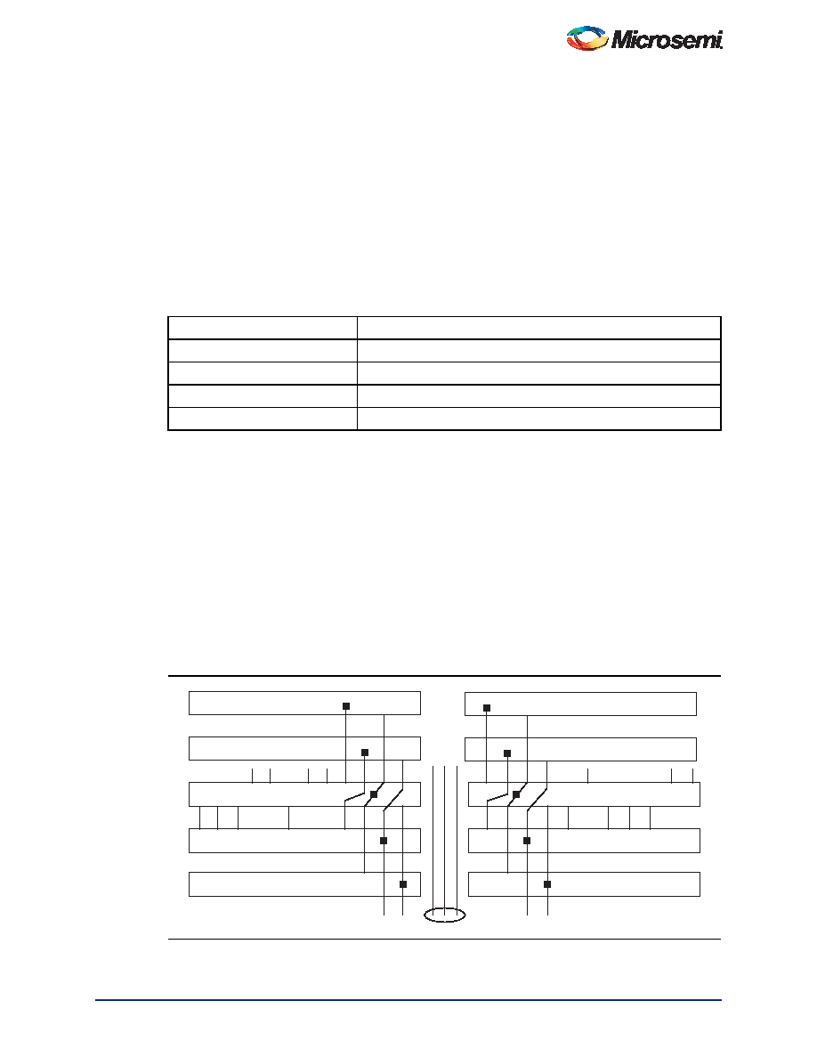
above and half of the inputs to segments in the channel below, as shown in Figure 2-9.
Table 2-1 Antifuse Types
Type
Description
XF
Horizontal-to-vertical connection
HF
Horizontal-to-horizontal connection
VF
Vertical-to-vertical connection
FF
"Fast" vertical connection
Figure 2-9
Logic Module Routing Interface
Y+2
Y+1
A1 D10 D11
B1 B0
D01 D00
Y-1
Y-2
LVTs
Y+2
Y+1
Y
Y-1
Y-2
C-Modules
S-Modules
D10
B0
A0 D11 A1
B1 D01
A0
Y
相关PDF资料 |
PDF描述 |
|---|---|
| A14V15A-PLG84C | IC FPGA 1500 GATES 3.3V 84-PLCC |
| 5745172-3 | CONN BACKSHELL DB15 DIE CAST |
| AFS250-1PQ208I | IC FPGA 2MB FLASH 250K 208PQFP |
| A10V10B-VQ80C | IC FPGA 1200 GATES 80-VQFP COM |
| 1-176793-0 | CONN SHIELD CASE .050 80POS WHT |
相关代理商/技术参数 |
参数描述 |
|---|---|
| A14V15A-PLG84C | 功能描述:IC FPGA 1500 GATES 3.3V 84-PLCC RoHS:是 类别:集成电路 (IC) >> 嵌入式 - FPGA(现场可编程门阵列) 系列:ACT™ 3 标准包装:40 系列:SX-A LAB/CLB数:6036 逻辑元件/单元数:- RAM 位总计:- 输入/输出数:360 门数:108000 电源电压:2.25 V ~ 5.25 V 安装类型:表面贴装 工作温度:0°C ~ 70°C 封装/外壳:484-BGA 供应商设备封装:484-FPBGA(27X27) |
| A14V15A-VQ100C | 功能描述:IC FPGA 1500 GATES 3.3V 100-VQFP RoHS:否 类别:集成电路 (IC) >> 嵌入式 - FPGA(现场可编程门阵列) 系列:ACT™ 3 标准包装:40 系列:SX-A LAB/CLB数:6036 逻辑元件/单元数:- RAM 位总计:- 输入/输出数:360 门数:108000 电源电压:2.25 V ~ 5.25 V 安装类型:表面贴装 工作温度:0°C ~ 70°C 封装/外壳:484-BGA 供应商设备封装:484-FPBGA(27X27) |
| A14V15A-VQG100C | 功能描述:IC FPGA 1500 GATES 3.3V 100-VQFP RoHS:是 类别:集成电路 (IC) >> 嵌入式 - FPGA(现场可编程门阵列) 系列:ACT™ 3 标准包装:40 系列:SX-A LAB/CLB数:6036 逻辑元件/单元数:- RAM 位总计:- 输入/输出数:360 门数:108000 电源电压:2.25 V ~ 5.25 V 安装类型:表面贴装 工作温度:0°C ~ 70°C 封装/外壳:484-BGA 供应商设备封装:484-FPBGA(27X27) |
| A14V25AA-1BG208B | 制造商:ACTEL 制造商全称:Actel Corporation 功能描述:Accelerator Series FPGAs - ACT 3Family |
| A14V25AA-1BG208C | 制造商:ACTEL 制造商全称:Actel Corporation 功能描述:Accelerator Series FPGAs - ACT 3Family |
发布紧急采购,3分钟左右您将得到回复。