- 您现在的位置:买卖IC网 > PDF目录364573 > A29002SERIES 256K X 8 Bit CMOS 5.0 Volt-only. Boot Sector Flash Memory PDF资料下载
参数资料
| 型号: | A29002SERIES |
| 英文描述: | 256K X 8 Bit CMOS 5.0 Volt-only. Boot Sector Flash Memory |
| 中文描述: | 256K × 8位CMOS 5.0伏特只。引导扇区闪存 |
| 文件页数: | 9/32页 |
| 文件大小: | 316K |
| 代理商: | A29002SERIES |
第1页第2页第3页第4页第5页第6页第7页第8页当前第9页第10页第11页第12页第13页第14页第15页第16页第17页第18页第19页第20页第21页第22页第23页第24页第25页第26页第27页第28页第29页第30页第31页第32页
A29001/A290011 Series
PRELIMINARY (December, 2002, Version 0.4)
9
AMIC Technology, Corp.
Chip Erase Command Sequence
Chip erase is a six-bus-cycle operation. The chip erase
command sequence is initiated by writing two unlock cycles,
followed by a set-up command. Two additional unlock write
cycles are then followed by the chip erase command, which
in turn invokes the Embedded Erase algorithm. The device
does not require the system to preprogram prior to erase.
The Embedded Erase algorithm automatically preprograms
and verifies the entire memory for an all zero data pattern
prior to electrical erase. The system is not required to provide
any controls or timings during these operations. The
Command Definitions table shows the address and data
requirements for the chip erase command sequence.
Any commands written to the chip during the Embedded
Erase algorithm are ignored. The system can determine the
status of the erase operation by using I/O
7
, I/O
6
, or I/O
2
. See
"Write Operation Status" for information on these status bits.
When the Embedded Erase algorithm is complete, the device
returns to reading array data and addresses are no longer
latched.
Figure 3 illustrates the algorithm for the erase operation. See
the Erase/Program Operations tables in "AC Characteristics"
for parameters, and to the Chip/Sector Erase Operation
Timings for timing waveforms.
Sector Erase Command Sequence
Sector erase is a six-bus-cycle operation. The sector erase
command sequence is initiated by writing two unlock cycles,
followed by a set-up command. Two additional unlock write
cycles are then followed by the address of the sector to be
erased, and the sector erase command. The Command
Definitions table shows the address and data requirements
for the sector erase command sequence.
The device does not require the system to preprogram the
memory prior to erase. The Embedded Erase algorithm
automatically programs and verifies the sector for an all zero
data pattern prior to electrical erase. The system is not
required to provide any controls or timings during these
operations.
After the command sequence is written, a sector erase time-
out of 50
μ
s begins. During the time-out period, additional
sector addresses and sector erase commands may be
written. Loading the sector erase buffer may be done in any
sequence, and the number of sectors may be from one
sector to all sectors. The time between these additional
cycles must be less than 50
μ
s, otherwise the last address
and command might not be accepted, and erasure may
begin. It is recommended that processor interrupts be
disabled during this time to ensure all commands are
accepted. The interrupts can be re-enabled after the last
Sector Erase command is written. If the time between
additional sector erase commands can be assumed to be
less than 50
μ
s, the system need not monitor I/O
3
. Any
command other than Sector Erase or Erase Suspend during
the time-out period resets the device to reading array data.
The system must rewrite the command sequence and any
additional sector addresses and commands.
The system can monitor I/O
3
to determine if the sector erase
timer has timed out. (See the " I/O
3
: Sector Erase Timer"
section.) The time-out begins from the rising edge of the final
WE
pulse in the command sequence.
Once the sector erase operation has begun, only the Erase
Suspend command is valid. All other commands are ignored.
When the Embedded Erase algorithm is complete, the device
returns to reading array data and addresses are no longer
latched. The system can determine the status of the erase
operation by using I/O
7
, I/O
6
, or I/O
2
. Refer to "Write
Operation Status" for information on these status bits.
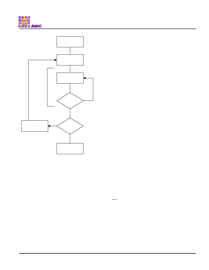
START
Write Program
Command
Sequence
Data Poll
from System
Verify Data
Last Address
Programming
Completed
No
Yes
Yes
Increment Address
Embedded
Program
algorithm in
progress
Note : See the appropriate Command Definitions table for
program command sequence.
Figure 2. Program Operation
相关PDF资料 |
PDF描述 |
|---|---|
| A29010SERIES | 128K X 8 Bit CMOS 5.0 Volt-only. Uniform Sector Flash Memory |
| A29040ASERIES | 512K X 8 Bit CMOS 5.0 Volt-only. Uniform Sector Flash Memory |
| A29040P-70 | IC-4M FLASH |
| A29040SERIES | 512K X 8 Bit CMOS 5.0 Volt-only. Uniform Sector Flash Memory |
| A2918EWH | Industrial Control IC |
相关代理商/技术参数 |
参数描述 |
|---|---|
| A29002T-120 | 制造商:AMICC 制造商全称:AMIC Technology 功能描述:256K X 8 Bit CMOS 5.0 Volt-only, Boot Sector Flash Memory |
| A29002T-150 | 制造商:AMICC 制造商全称:AMIC Technology 功能描述:256K X 8 Bit CMOS 5.0 Volt-only, Boot Sector Flash Memory |
| A29002T-55 | 制造商:AMICC 制造商全称:AMIC Technology 功能描述:256K X 8 Bit CMOS 5.0 Volt-only, Boot Sector Flash Memory |
| A29002T-70 | 制造商:AMICC 制造商全称:AMIC Technology 功能描述:256K X 8 Bit CMOS 5.0 Volt-only, Boot Sector Flash Memory |
| A29002T-90 | 制造商:AMICC 制造商全称:AMIC Technology 功能描述:256K X 8 Bit CMOS 5.0 Volt-only, Boot Sector Flash Memory |
发布紧急采购,3分钟左右您将得到回复。