- 您现在的位置:买卖IC网 > PDF目录209982 > A3P030-2QNG68II FPGA, 768 CLBS, 30000 GATES, 350 MHz, QCC68 PDF资料下载
参数资料
| 型号: | A3P030-2QNG68II |
| 元件分类: | FPGA |
| 英文描述: | FPGA, 768 CLBS, 30000 GATES, 350 MHz, QCC68 |
| 封装: | 8 X 8 MM, 0.90 MM HEIGHT, 0.40 MM PITCH, GREEN, QFN-68 |
| 文件页数: | 29/49页 |
| 文件大小: | 5893K |
| 代理商: | A3P030-2QNG68II |
第1页第2页第3页第4页第5页第6页第7页第8页第9页第10页第11页第12页第13页第14页第15页第16页第17页第18页第19页第20页第21页第22页第23页第24页第25页第26页第27页第28页当前第29页第30页第31页第32页第33页第34页第35页第36页第37页第38页第39页第40页第41页第42页第43页第44页第45页第46页第47页第48页第49页
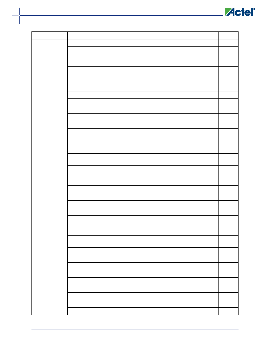
ProASIC3 DC and Switching Characteristics
2- 108
v1.3
Advance v0.3
M7 device information is new.
N/A
Table 2-4 ProASIC3 Globals/Spines/Rows by Device was updated to include the
number or rows in each top or bottom spine.
2-16
EXTFB was removed from Figure 2-24 ProASIC3E CCC Options.
2-24
The "PLL Macro" section was updated. EXTFB information was removed from
this section.
2-15
The CCC Output Peak-to-Peak Period Jitter FCCC_OUT was updated in Table 2-
11 ProASIC3 CCC/PLL Specification
2-29
EXTFB was removed from Figure 2-27 CCC/PLL Macro.
2-28
Table 2-13 ProASIC3 I/O Features was updated.
2-30
The "Hot-Swap Support" section was updated.
2-33
The "Cold-Sparing Support" section was updated.
2-34
"Electrostatic Discharge (ESD) Protection" section was updated.
2-35
The LVPECL specification in Table 2-43 I/O Hot-Swap and 5 V Input Tolerance
Capabilities in ProASIC3 Devices was updated.
2-64
In the Bank 1 area of Figure 2-72, VMV2 was changed to VMV1 and VCCIB2 was
changed to VCCIB1.
2-97
The VJTAG and I/O pin descriptions were updated in the "Pin Descriptions"
section.
2-50
The "JTAG Pins" section was updated.
2-51
"128-Bit AES Decryption" section was updated to include M7 device
information.
2-53
Table 3-6 was updated.
3-6
Table 3-7 was updated.
3-6
In Table 3-11, PAC4 was updated.
3-93-8
Table 3-20 was updated.
3-20
The note in Table 3-32 was updated.
3-27
All Timing Characteristics tables were updated from LVTTL to Register Delays
3-31 to
3-73
The Timing Characteristics for RAM4K9, RAM512X18, and FIFO were updated.
3-85 to
3-90
FTCKMAX was updated in Table 3-110.
3-97
Advance v0.2
Figure 2-11 was updated.
2-9
The "Clock Resources (VersaNets)" section was updated.
2-9
The "VersaNet Global Networks and Spine Access" section was updated.
2-9
The "PLL Macro" section was updated.
2-15
Figure 2-27 was updated.
2-28
Figure 2-20 was updated.
2-19
Table 2-5 was updated.
2-25
Table 2-6 was updated.
2-25
Previous Version
Changes in Current Version (v1.3)
Page
相关PDF资料 |
PDF描述 |
|---|---|
| A3P030-2VQ100II | FPGA, 768 CLBS, 30000 GATES, 350 MHz, PQFP100 |
| A3P030-2VQG100II | FPGA, 768 CLBS, 30000 GATES, 350 MHz, PQFP100 |
| A3P030-FQN48 | FPGA, 768 CLBS, 30000 GATES, 350 MHz, QCC48 |
| A3P030-FQN68 | FPGA, 768 CLBS, 30000 GATES, 350 MHz, QCC68 |
| A3P030-FQNG48 | FPGA, 768 CLBS, 30000 GATES, 350 MHz, QCC48 |
相关代理商/技术参数 |
参数描述 |
|---|---|
| A3P030-2VQ100 | 功能描述:IC FPGA 1KB FLASH 30K 100-VQFP RoHS:否 类别:集成电路 (IC) >> 嵌入式 - FPGA(现场可编程门阵列) 系列:ProASIC3 标准包装:152 系列:IGLOO PLUS LAB/CLB数:- 逻辑元件/单元数:792 RAM 位总计:- 输入/输出数:120 门数:30000 电源电压:1.14 V ~ 1.575 V 安装类型:表面贴装 工作温度:-40°C ~ 85°C 封装/外壳:289-TFBGA,CSBGA 供应商设备封装:289-CSP(14x14) |
| A3P030-2VQ100I | 功能描述:IC FPGA 1KB FLASH 30K 100-VQFP RoHS:否 类别:集成电路 (IC) >> 嵌入式 - FPGA(现场可编程门阵列) 系列:ProASIC3 标准包装:152 系列:IGLOO PLUS LAB/CLB数:- 逻辑元件/单元数:792 RAM 位总计:- 输入/输出数:120 门数:30000 电源电压:1.14 V ~ 1.575 V 安装类型:表面贴装 工作温度:-40°C ~ 85°C 封装/外壳:289-TFBGA,CSBGA 供应商设备封装:289-CSP(14x14) |
| A3P030-2VQ144 | 制造商:ACTEL 制造商全称:Actel Corporation 功能描述:ProASIC3 Flash Family FPGAs |
| A3P030-2VQ144ES | 制造商:ACTEL 制造商全称:Actel Corporation 功能描述:ProASIC3 Flash Family FPGAs |
| A3P030-2VQ144I | 制造商:ACTEL 制造商全称:Actel Corporation 功能描述:ProASIC3 Flash Family FPGAs |
发布紧急采购,3分钟左右您将得到回复。