- 您现在的位置:买卖IC网 > PDF目录209983 > A3P030-FQN132 FPGA, 768 CLBS, 30000 GATES, 350 MHz, BCC132 PDF资料下载
参数资料
| 型号: | A3P030-FQN132 |
| 元件分类: | FPGA |
| 英文描述: | FPGA, 768 CLBS, 30000 GATES, 350 MHz, BCC132 |
| 封装: | 8 X 8 MM, 0.75 MM HEIGHT, 0.50 MM PITCH, QFN-132 |
| 文件页数: | 28/49页 |
| 文件大小: | 5893K |
| 代理商: | A3P030-FQN132 |
第1页第2页第3页第4页第5页第6页第7页第8页第9页第10页第11页第12页第13页第14页第15页第16页第17页第18页第19页第20页第21页第22页第23页第24页第25页第26页第27页当前第28页第29页第30页第31页第32页第33页第34页第35页第36页第37页第38页第39页第40页第41页第42页第43页第44页第45页第46页第47页第48页第49页
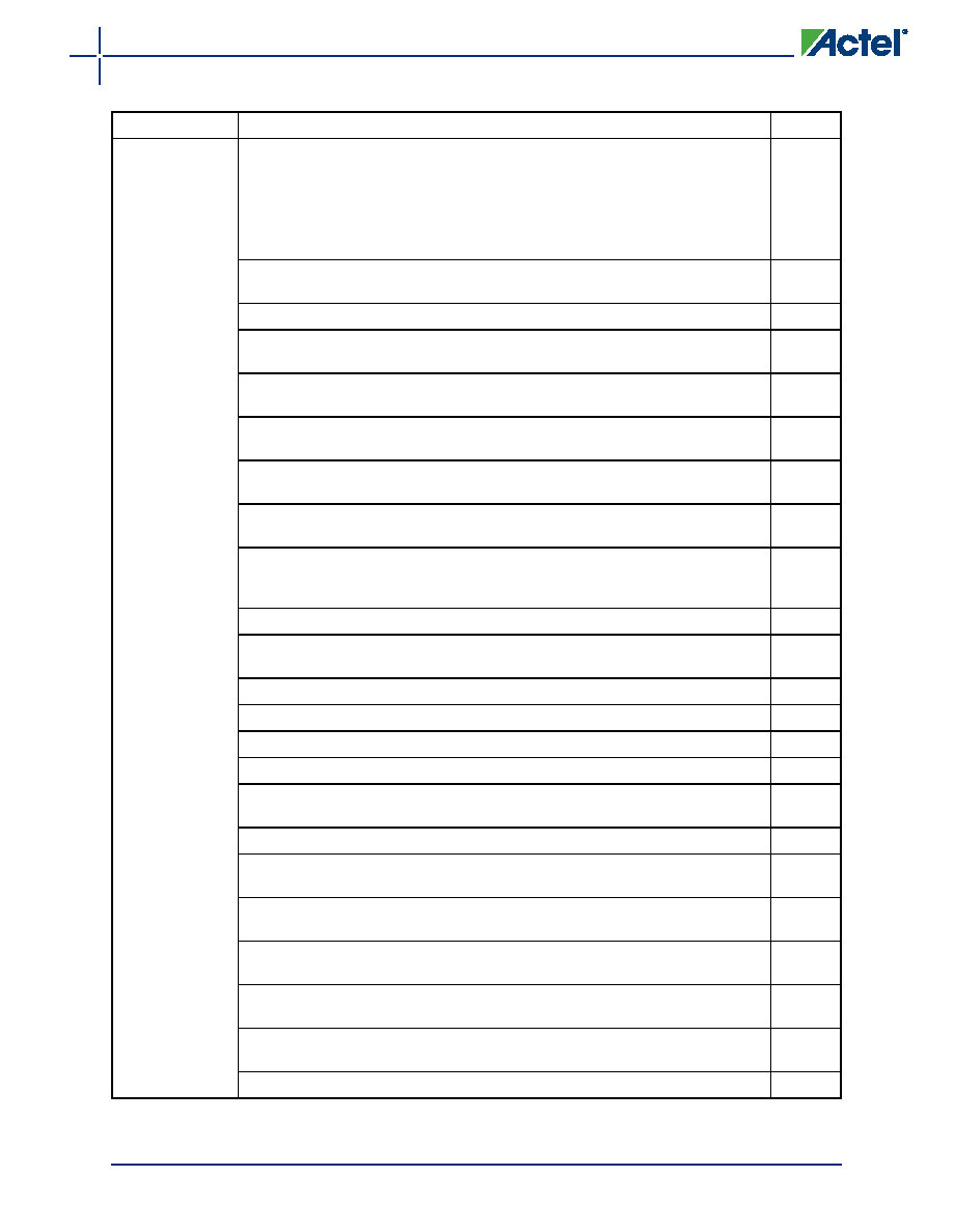
ProASIC3 DC and Switching Characteristics
v1.3
2 - 107
Advance v0.5
(continued)
The "I/O Banks" section is new. This section explains the following types of I/Os:
Advanced
Standard+
Standard
Table 2-12 Automotive ProASIC3 Bank Types Definition and Differences is
new. This table describes the standards listed above.
2-29
PCI-X 3.3 V was added to the Compatible Standards for 3.3 V in Table 2-
11 VCCI Voltages and Compatible Standards
2-29
Table 2-13 ProASIC3 I/O Features was updated.
2-30
The "Double Data Rate (DDR) Support" section was updated to include
information concerning implementation of the feature.
2-32
The "Electrostatic Discharge (ESD) Protection" section was updated to include
testing information.
2-35
Level 3 and 4 descriptions were updated in Table 2-43 I/O Hot-Swap and 5 V
Input Tolerance Capabilities in ProASIC3 Devices.
2-64
The notes in Table 2-43 I/O Hot-Swap and 5 V Input Tolerance Capabilities in
ProASIC3 Devices were updated.
2-64
The "Simultaneous Switching Outputs (SSOs) and Printed Circuit Board Layout"
section is new.
2-41
A footnote was added to Table 2-14 Maximum I/O Frequency for Single-Ended
and Differential I/Os in All Banks in Automotive ProASIC3 Devices (maximum
drive strength and high slew selected).
2-30
Table 2-18 Automotive ProASIC3 I/O Attributes vs. I/O Standard Applications
2-45
Table 2-50 ProASIC3 Output Drive (OUT_DRIVE) for Standard I/O Bank Type
(A3P030 device)
2-83
Table 2-51 ProASIC3 Output Drive for Standard+ I/O Bank Type was updated.
2-84
Table 2-54 ProASIC3 Output Drive for Advanced I/O Bank Type was updated.
2-84
The "x" was updated in the "User I/O Naming Convention" section.
2-48
The "VCC Core Supply Voltage" pin description was updated.
2-50
The "VMVx I/O Supply Voltage (quiet)" pin description was updated to include
information concerning leaving the pin unconnected.
2-50
The "VJTAG JTAG Supply Voltage" pin description was updated.
2-50
The "VPUMP Programming Supply Voltage" pin description was updated to
include information on what happens when the pin is tied to ground.
2-50
The "I/O User Input/Output" pin description was updated to include information
on what happens when the pin is unused.
2-50
The "JTAG Pins" section was updated to include information on what happens
when the pin is unused.
2-51
The "Programming" section was updated to include information concerning
serialization.
2-53
The
"JTAG
1532"
section
was
updated
to
include
SAMPLE/PRELOAD
information.
2-54
"DC and Switching Characteristics" chapter was updated with new information.
3-1
Previous Version
Changes in Current Version (v1.3)
Page
相关PDF资料 |
PDF描述 |
|---|---|
| A3P030-FVQ100 | FPGA, 768 CLBS, 30000 GATES, 350 MHz, PQFP100 |
| A3P125-FFG144 | FPGA, 3072 CLBS, 125000 GATES, 350 MHz, PBGA144 |
| A3P125-FPQ208 | FPGA, 3072 CLBS, 125000 GATES, 350 MHz, PQFP208 |
| A3P125-FTQ144 | FPGA, 3072 CLBS, 125000 GATES, 350 MHz, PQFP144 |
| A3P125-FVQ100 | FPGA, 3072 CLBS, 125000 GATES, 350 MHz, PQFP100 |
相关代理商/技术参数 |
参数描述 |
|---|---|
| A3P030-FQNG132 | 制造商:Microsemi Corporation 功能描述:FPGA PROASIC3 30K GATES 193MHZ 130NM 1.5V 132QFN - Trays |
| A3P030-FVQ100 | 制造商:Microsemi Corporation 功能描述:FPGA PROASIC3 30K GATES 193MHZ 130NM 1.5V 100VQFP - Trays |
| A3P030-FVQ144 | 制造商:ACTEL 制造商全称:Actel Corporation 功能描述:ProASIC3 Flash Family FPGAs |
| A3P030-FVQ144ES | 制造商:ACTEL 制造商全称:Actel Corporation 功能描述:ProASIC3 Flash Family FPGAs |
| A3P030-FVQ144I | 制造商:ACTEL 制造商全称:Actel Corporation 功能描述:ProASIC3 Flash Family FPGAs |
发布紧急采购,3分钟左右您将得到回复。