- 您现在的位置:买卖IC网 > PDF目录253906 > A3P1000-FFGG144 FPGA, 24576 CLBS, 1000000 GATES, 350 MHz, PBGA144 PDF资料下载
参数资料
| 型号: | A3P1000-FFGG144 |
| 元件分类: | FPGA |
| 英文描述: | FPGA, 24576 CLBS, 1000000 GATES, 350 MHz, PBGA144 |
| 封装: | 13X 13 MM, 1.45 MM HEIGHT, 1 MM PITCH, GREEN, FBGA-144 |
| 文件页数: | 46/49页 |
| 文件大小: | 5893K |
| 代理商: | A3P1000-FFGG144 |
第1页第2页第3页第4页第5页第6页第7页第8页第9页第10页第11页第12页第13页第14页第15页第16页第17页第18页第19页第20页第21页第22页第23页第24页第25页第26页第27页第28页第29页第30页第31页第32页第33页第34页第35页第36页第37页第38页第39页第40页第41页第42页第43页第44页第45页当前第46页第47页第48页第49页
ProASIC3 DC and Switching Characteristics
v1.3
2 - 79
Global Tree Timing Characteristics
Global clock delays include the central rib delay, the spine delay, and the row delay. Delays do not
include I/O input buffer clock delays, as these are I/O standard–dependent, and the clock may be
driven and conditioned internally by the CCC module. For more details on clock conditioning
capabilities, refer to the "Clock Conditioning Circuits" section on page 2-83. Table 2-99 to
Table 2-105 on page 2-82 present minimum and maximum global clock delays within each device.
Minimum and maximum delays are measured with minimum and maximum loading.
Timing Characteristics
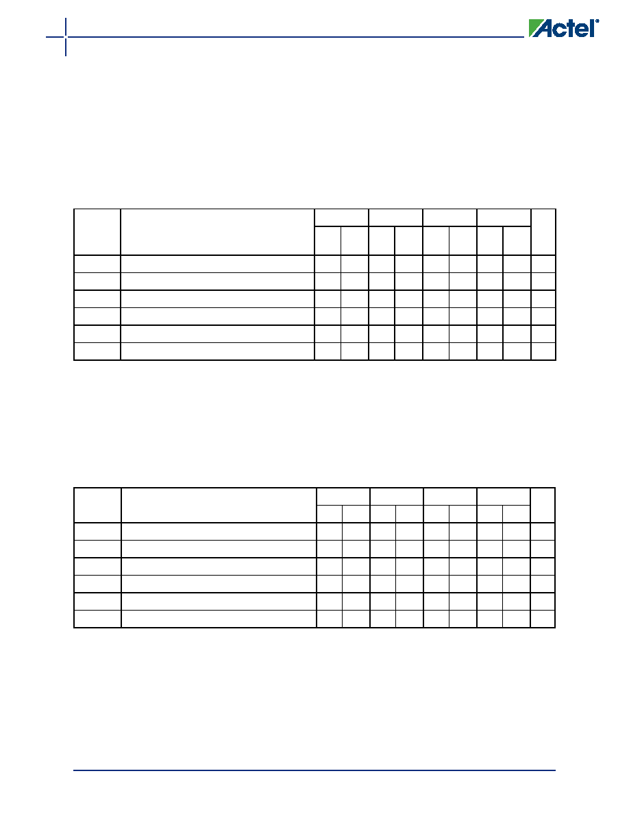
Table 2-98 A3P015 Global Resource
Commercial-Case Conditions: TJ = 70°C, VCC = 1.425 V
Parameter Description
–2
–1
Std.
–F
Units
Min.1 Max.2 Min.1 Max.2 Min.1 Max.2 Min.1 Max.2
tRCKL
Input LOW Delay for Global Clock
0.66
0.81
0.75
0.92
0.88
1.08
1.06
1.30
ns
tRCKH
Input HIGH Delay for Global Clock
0.67
0.84
0.76
0.96
0.89
1.13
1.07
1.36
ns
tRCKMPWH Minimum Pulse Width HIGH for Global Clock
ns
tRCKMPWL Minimum Pulse Width LOW for Global Clock
ns
tRCKSW
Maximum Skew for Global Clock
0.18
0.21
0.25
0.30
ns
FRMAX
Maximum Frequency for Global Clock
MHz
Notes:
1. Value reflects minimum load. The delay is measured from the CCC output to the clock pin of a sequential
element, located in a lightly loaded row (single element is connected to the global net).
2. Value reflects maximum load. The delay is measured on the clock pin of the farthest sequential element,
located in a fully loaded row (all available flip-flops are connected to the global net in the row).
3. For specific junction temperature and voltage-supply levels, refer to Table 2-6 on page 2-6 for derating
values.
Table 2-99 A3P030 Global Resource
Commercial-Case Conditions: TJ = 70°C, VCC = 1.425 V
Parameter
Description
–2
–1
Std.
–F
Units
Min.1 Max.2 Min.1 Max.2 Min.1 Max.2 Min.1 Max.2
tRCKL
Input LOW Delay for Global Clock
0.67 0.81 0.76 0.92 0.89 1.09 1.07 1.31
ns
tRCKH
Input HIGH Delay for Global Clock
0.680.85 0.770.970.911.141.091.37
ns
tRCKMPWH Minimum Pulse Width HIGH for Global Clock
ns
tRCKMPWL Minimum Pulse Width LOW for Global Clock
ns
tRCKSW
Maximum Skew for Global Clock
0.18
0.21
0.24
0.29
ns
FRMAX
Maximum Frequency for Global Clock
MHz
Notes:
1. Value reflects minimum load. The delay is measured from the CCC output to the clock pin of a sequential
element, located in a lightly loaded row (single element is connected to the global net).
2. Value reflects maximum load. The delay is measured on the clock pin of the farthest sequential element,
located in a fully loaded row (all available flip-flops are connected to the global net in the row).
3. For specific junction temperature and voltage supply levels, refer to Table 2-6 on page 2-6 for derating
values.
相关PDF资料 |
PDF描述 |
|---|---|
| A3P1000-FFGG256 | FPGA, 24576 CLBS, 1000000 GATES, 350 MHz, PBGA256 |
| A3P1000-FFGG484 | FPGA, 24576 CLBS, 1000000 GATES, 350 MHz, PBGA484 |
| A3P1000-FPQG208 | FPGA, 24576 CLBS, 1000000 GATES, 350 MHz, PQFP208 |
| ATL80/50-256AM | FPGA, 30000 GATES |
| ATL80/50-256QM | FPGA, 30000 GATES |
相关代理商/技术参数 |
参数描述 |
|---|---|
| A3P1000-FFGG144ES | 制造商:ACTEL 制造商全称:Actel Corporation 功能描述:ProASIC3 Flash Family FPGAs |
| A3P1000-FFGG144I | 制造商:ACTEL 制造商全称:Actel Corporation 功能描述:ProASIC3 Flash Family FPGAs |
| A3P1000-FFGG144PP | 制造商:ACTEL 制造商全称:Actel Corporation 功能描述:ProASIC3 Flash Family FPGAs |
| A3P1000-FFGG256 | 制造商:Microsemi Corporation 功能描述:FPGA PROASIC3 1M GATES 193MHZ COMM 130NM 1.5V 256FBGA - Trays |
| A3P1000-FFGG484 | 制造商:Microsemi Corporation 功能描述:FPGA PROASIC3 1M GATES 193MHZ COMM 130NM 1.5V 484FBGA - Trays |
发布紧急采购,3分钟左右您将得到回复。