- 您现在的位置:买卖IC网 > PDF目录209983 > A3P125-TQG144II FPGA, 3072 CLBS, 125000 GATES, 350 MHz, PQFP144 PDF资料下载
参数资料
| 型号: | A3P125-TQG144II |
| 元件分类: | FPGA |
| 英文描述: | FPGA, 3072 CLBS, 125000 GATES, 350 MHz, PQFP144 |
| 封装: | 20 X 20 MM, 1.40 MM HEIGHT, 0.50 MM PITCH, GREEN, TQFP-144 |
| 文件页数: | 33/49页 |
| 文件大小: | 5893K |
| 代理商: | A3P125-TQG144II |
第1页第2页第3页第4页第5页第6页第7页第8页第9页第10页第11页第12页第13页第14页第15页第16页第17页第18页第19页第20页第21页第22页第23页第24页第25页第26页第27页第28页第29页第30页第31页第32页当前第33页第34页第35页第36页第37页第38页第39页第40页第41页第42页第43页第44页第45页第46页第47页第48页第49页
ProASIC3 DC and Switching Characteristics
v1.3
2 - 77
Timing Characteristics
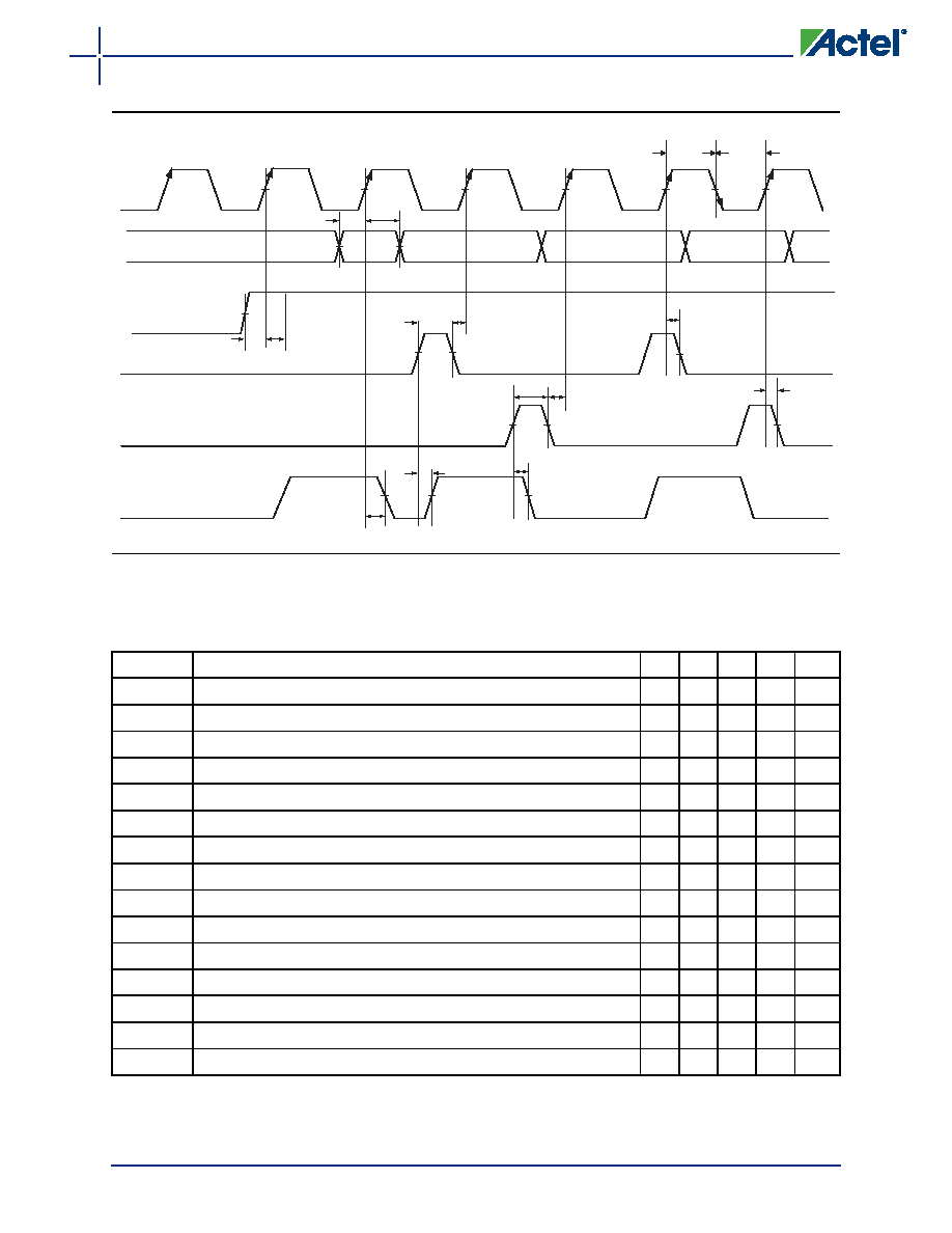
Figure 2-26 Timing Model and Waveforms
PRE
CLR
Out
CLK
Data
EN
tSUE
50%
tSUD
tHD
50%
tCLKQ
0
tHE
tRECPRE
tREMPRE
tRECCLR
tREMCLR
tWCLR
tWPRE
tPRE2Q
tCLR2Q
tCKMPWHtCKMPWL
50%
Table 2-97 Register Delays
Commercial-Case Conditions: TJ = 70°C, Worst-Case VCC = 1.425 V
Parameter
Description
–2
–1
Std.
–F
Units
tCLKQ
Clock-to-Q of the Core Register
0.55 0.63 0.74 0.89
ns
tSUD
Data Setup Time for the Core Register
0.43 0.49 0.57 0.69
ns
tHD
Data Hold Time for the Core Register
0.00 0.00 0.00 0.00
ns
tSUE
Enable Setup Time for the Core Register
0.45 0.52 0.61 0.73
ns
tHE
Enable Hold Time for the Core Register
0.00 0.00 0.00 0.00
ns
tCLR2Q
Asynchronous Clear-to-Q of the Core Register
0.40 0.45 0.53 0.64
ns
tPRE2Q
Asynchronous Preset-to-Q of the Core Register
0.40 0.45 0.53 0.64
ns
tREMCLR
Asynchronous Clear Removal Time for the Core Register
0.00 0.00 0.00 0.00
ns
tRECCLR
Asynchronous Clear Recovery Time for the Core Register
0.22 0.25 0.30 0.36
ns
tREMPRE
Asynchronous Preset Removal Time for the Core Register
0.00 0.00 0.00 0.00
ns
tRECPRE
Asynchronous Preset Recovery Time for the Core Register
0.22 0.25 0.30 0.36
ns
tWCLR
Asynchronous Clear Minimum Pulse Width for the Core Register
0.22 0.25 0.30 0.36
ns
tWPRE
Asynchronous Preset Minimum Pulse Width for the Core Register
0.22 0.25 0.30 0.36
ns
tCKMPWH
Clock Minimum Pulse Width HIGH for the Core Register
0.32 0.37 0.43 0.52
ns
tCKMPWL
Clock Minimum Pulse Width LOW for the Core Register
0.36 0.41 0.48 0.57
ns
Note: For specific junction temperature and voltage supply levels, refer to Table 2-6 on page 2-6 for derating
values.
相关PDF资料 |
PDF描述 |
|---|---|
| A3P125-VQ100II | FPGA, 3072 CLBS, 125000 GATES, 350 MHz, PQFP100 |
| A3P125-VQG100II | FPGA, 3072 CLBS, 125000 GATES, 350 MHz, PQFP100 |
| A42MX36-3PQG208B | FPGA, 2438 CLBS, 36000 GATES, PQFP208 |
| A3P030-FQN132 | FPGA, 768 CLBS, 30000 GATES, 350 MHz, BCC132 |
| A3P030-FVQ100 | FPGA, 768 CLBS, 30000 GATES, 350 MHz, PQFP100 |
相关代理商/技术参数 |
参数描述 |
|---|---|
| A3P125-VQ100 | 功能描述:IC FPGA 1KB FLASH 125K 100-VQFP RoHS:否 类别:集成电路 (IC) >> 嵌入式 - FPGA(现场可编程门阵列) 系列:ProASIC3 标准包装:152 系列:IGLOO PLUS LAB/CLB数:- 逻辑元件/单元数:792 RAM 位总计:- 输入/输出数:120 门数:30000 电源电压:1.14 V ~ 1.575 V 安装类型:表面贴装 工作温度:-40°C ~ 85°C 封装/外壳:289-TFBGA,CSBGA 供应商设备封装:289-CSP(14x14) |
| A3P125-VQ100I | 功能描述:IC FPGA 1KB FLASH 125K 100-VQFP RoHS:否 类别:集成电路 (IC) >> 嵌入式 - FPGA(现场可编程门阵列) 系列:ProASIC3 标准包装:152 系列:IGLOO PLUS LAB/CLB数:- 逻辑元件/单元数:792 RAM 位总计:- 输入/输出数:120 门数:30000 电源电压:1.14 V ~ 1.575 V 安装类型:表面贴装 工作温度:-40°C ~ 85°C 封装/外壳:289-TFBGA,CSBGA 供应商设备封装:289-CSP(14x14) |
| A3P125-VQ100T | 功能描述:IC FPGA 1KB FLASH 125K 100-VQFP RoHS:否 类别:集成电路 (IC) >> 嵌入式 - FPGA(现场可编程门阵列) 系列:ProASIC3 标准包装:152 系列:IGLOO PLUS LAB/CLB数:- 逻辑元件/单元数:792 RAM 位总计:- 输入/输出数:120 门数:30000 电源电压:1.14 V ~ 1.575 V 安装类型:表面贴装 工作温度:-40°C ~ 85°C 封装/外壳:289-TFBGA,CSBGA 供应商设备封装:289-CSP(14x14) |
| A3P125-VQ144 | 制造商:ACTEL 制造商全称:Actel Corporation 功能描述:ProASIC3 Flash Family FPGAs |
| A3P125-VQ144ES | 制造商:ACTEL 制造商全称:Actel Corporation 功能描述:ProASIC3 Flash Family FPGAs |
发布紧急采购,3分钟左右您将得到回复。