参数资料
| 型号: | A3P600L-PQG208I |
| 厂商: | Microsemi SoC |
| 文件页数: | 237/242页 |
| 文件大小: | 0K |
| 描述: | IC FPGA 1KB FLASH 600K 208-PQFP |
| 标准包装: | 24 |
| 系列: | ProASIC3L |
| RAM 位总计: | 110592 |
| 输入/输出数: | 154 |
| 门数: | 600000 |
| 电源电压: | 1.14V ~ 1.575 V |
| 安装类型: | 表面贴装 |
| 工作温度: | -40°C ~ 85°C |
| 封装/外壳: | 208-BFQFP |
| 供应商设备封装: | 208-PQFP(28x28) |
第1页第2页第3页第4页第5页第6页第7页第8页第9页第10页第11页第12页第13页第14页第15页第16页第17页第18页第19页第20页第21页第22页第23页第24页第25页第26页第27页第28页第29页第30页第31页第32页第33页第34页第35页第36页第37页第38页第39页第40页第41页第42页第43页第44页第45页第46页第47页第48页第49页第50页第51页第52页第53页第54页第55页第56页第57页第58页第59页第60页第61页第62页第63页第64页第65页第66页第67页第68页第69页第70页第71页第72页第73页第74页第75页第76页第77页第78页第79页第80页第81页第82页第83页第84页第85页第86页第87页第88页第89页第90页第91页第92页第93页第94页第95页第96页第97页第98页第99页第100页第101页第102页第103页第104页第105页第106页第107页第108页第109页第110页第111页第112页第113页第114页第115页第116页第117页第118页第119页第120页第121页第122页第123页第124页第125页第126页第127页第128页第129页第130页第131页第132页第133页第134页第135页第136页第137页第138页第139页第140页第141页第142页第143页第144页第145页第146页第147页第148页第149页第150页第151页第152页第153页第154页第155页第156页第157页第158页第159页第160页第161页第162页第163页第164页第165页第166页第167页第168页第169页第170页第171页第172页第173页第174页第175页第176页第177页第178页第179页第180页第181页第182页第183页第184页第185页第186页第187页第188页第189页第190页第191页第192页第193页第194页第195页第196页第197页第198页第199页第200页第201页第202页第203页第204页第205页第206页第207页第208页第209页第210页第211页第212页第213页第214页第215页第216页第217页第218页第219页第220页第221页第222页第223页第224页第225页第226页第227页第228页第229页第230页第231页第232页第233页第234页第235页第236页当前第237页第238页第239页第240页第241页第242页
ProASIC3L DC and Switching Characteristics
2-78
Revision 13
Timing Characteristics
1.2 V DC Core Voltage
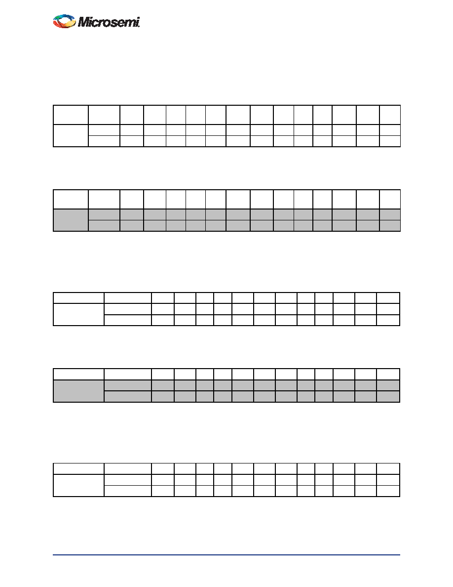
Table 2-117 1.2 V LVCMOS Low Slew
Commercial-Case Conditions: TJ = 70°C, Worst-Case VCC = 1.425 V, Worst-Case VCCI = 1.4 V
Applicable to Pro I/O Banks
Drive
Strength
Speed
Grade
tDOUT
tDP
tDIN
tPY
tPYS tEOUT
tZL
tZH
tLZ
tHZ
tZLS
tZHS
Unit
s
2 mA
Std.
0.77
11.80 0.05 2.38 3.52
0.50
10.97 8.61 4.79 4.38 12.91 10.55
ns
–1
0.66
10.04 0.04 2.02 2.99
0.43
9.33
7.32 4.08 3.72 10.98
8.97
ns
Note: For specific junction temperature and voltage supply levels, refer to Table 2-6 on page 2-7 for derating values.
Table 2-118 1.2 V LVCMOS High Slew
Commercial-Case Conditions: TJ = 70°C, Worst-Case VCC = 1.425 V, Worst-Case VCCI = 1.4 V
Applicable to Pro I/O Banks
Drive
Strength
Speed
Grade
tDOUT
tDP
tDIN
tPY
tPYS tEOUT
tZL
tZH
tLZ
tHZ
tZLS
tZHS
Unit
s
2 mA
Std.
0.77
4.84
0.05 2.38 3.52
0.50
4.50
3.96 4.78 4.51
6.44
5.90
ns
–1
0.66
4.12
0.04 2.02 2.99
0.43
3.83
3.37 4.06 3.84
5.48
5.02
ns
Notes:
1. Software default selection highlighted in gray.
2. For specific junction temperature and voltage supply levels, refer to Table 2-6 on page 2-7 for derating values.
Table 2-119 1.2 V LVCMOS High Slew
Commercial-Case Conditions: TJ = 70°C, Worst-Case VCC = 1.14 V, Worst-Case VCCI = 1.14 V
Applicable to Advanced I/O Banks
Drive Strength Speed Grade tDOUT tDP
tDIN tPY tEOUT
tZL
tZH
tLZ
tHZ
tZLS
tZHS Units
2 mA
Std.
0.70
8.77 0.05 1.82 0.50
6.17
5.45 2.80 2.77 8.11
7.39
ns
–1
0.60
7.46 0.04 1.55 0.43
5.25
4.63 2.39 2.35 6.90
6.28
ns
Note: For specific junction temperature and voltage supply levels, refer to Table 2-6 on page 2-7 for derating values.
Table 2-120 1.2 V LVCMOS High Slew
Commercial-Case Conditions: TJ = 70°C, Worst-Case VCC = 1.14 V, Worst-Case VCCI = 1.14 V
Applicable to Advanced I/O Banks
Drive Strength Speed Grade tDOUT tDP
tDIN tPY tEOUT
tZL
tZH
tLZ
tHZ
tZLS
tZHS Units
2 mA
Std.
0.70
3.73 0.05 1.82 0.50
2.48
2.06 2.80 2.89 4.42
4.00
ns
–1
0.60
3.17 0.04 1.55 0.43
2.11
1.76 2.38 2.46 3.76
3.41
ns
Notes:
1. Software default selection highlighted in gray.
2. For specific junction temperature and voltage supply levels, refer to Table 2-6 on page 2-7 for derating values.
Table 2-121 1.2 V LVCMOS High Slew
Commercial-Case Conditions: TJ = 70°C, Worst-Case VCC = 1.14 V, Worst-Case VCCI = 1.14 V
Applicable to Standard Plus I/O Banks
Drive Strength Speed Grade tDOUT tDP
tDIN tPY tEOUT
tZL
tZH
tLZ
tHZ
tZLS
tZHS Units
2 mA
Std.
0.70
9.67 0.05 1.83 0.50
6.78
5.99 4.08 4.57 8.72
7.93
ns
–1
0.60
8.23 0.04 1.56 0.43
5.77
5.09 3.47 3.88 7.42
6.74
ns
Note: For specific junction temperature and voltage supply levels, refer to Table 2-6 on page 2-7 for derating values.
相关PDF资料 |
PDF描述 |
|---|---|
| A3P600L-PQ208I | IC FPGA 1KB FLASH 600K 208-PQFP |
| M1A3P600-2PQG208I | IC FPGA 1KB FLASH 600K 208-PQFP |
| M1A3P600L-PQG208I | IC FPGA 1KB FLASH 600K 208-PQFP |
| M1A3P600-2PQ208I | IC FPGA 1KB FLASH 600K 208-PQFP |
| EP20K100EQC208-3 | IC APEX 20KE FPGA 100K 208-PQFP |
相关代理商/技术参数 |
参数描述 |
|---|---|
| A3P600-PQ144 | 制造商:ACTEL 制造商全称:Actel Corporation 功能描述:ProASIC3 Flash Family FPGAs |
| A3P600-PQ144ES | 制造商:ACTEL 制造商全称:Actel Corporation 功能描述:ProASIC3 Flash Family FPGAs |
| A3P600-PQ144I | 制造商:ACTEL 制造商全称:Actel Corporation 功能描述:ProASIC3 Flash Family FPGAs |
| A3P600-PQ144PP | 制造商:ACTEL 制造商全称:Actel Corporation 功能描述:ProASIC3 Flash Family FPGAs |
| A3P600-PQ208 | 功能描述:IC FPGA 1KB FLASH 600K 208-PQFP RoHS:否 类别:集成电路 (IC) >> 嵌入式 - FPGA(现场可编程门阵列) 系列:ProASIC3 标准包装:90 系列:ProASIC3 LAB/CLB数:- 逻辑元件/单元数:- RAM 位总计:36864 输入/输出数:157 门数:250000 电源电压:1.425 V ~ 1.575 V 安装类型:表面贴装 工作温度:-40°C ~ 125°C 封装/外壳:256-LBGA 供应商设备封装:256-FPBGA(17x17) |
发布紧急采购,3分钟左右您将得到回复。