参数资料
| 型号: | A3P600L-PQG208I |
| 厂商: | Microsemi SoC |
| 文件页数: | 51/242页 |
| 文件大小: | 0K |
| 描述: | IC FPGA 1KB FLASH 600K 208-PQFP |
| 标准包装: | 24 |
| 系列: | ProASIC3L |
| RAM 位总计: | 110592 |
| 输入/输出数: | 154 |
| 门数: | 600000 |
| 电源电压: | 1.14V ~ 1.575 V |
| 安装类型: | 表面贴装 |
| 工作温度: | -40°C ~ 85°C |
| 封装/外壳: | 208-BFQFP |
| 供应商设备封装: | 208-PQFP(28x28) |
第1页第2页第3页第4页第5页第6页第7页第8页第9页第10页第11页第12页第13页第14页第15页第16页第17页第18页第19页第20页第21页第22页第23页第24页第25页第26页第27页第28页第29页第30页第31页第32页第33页第34页第35页第36页第37页第38页第39页第40页第41页第42页第43页第44页第45页第46页第47页第48页第49页第50页当前第51页第52页第53页第54页第55页第56页第57页第58页第59页第60页第61页第62页第63页第64页第65页第66页第67页第68页第69页第70页第71页第72页第73页第74页第75页第76页第77页第78页第79页第80页第81页第82页第83页第84页第85页第86页第87页第88页第89页第90页第91页第92页第93页第94页第95页第96页第97页第98页第99页第100页第101页第102页第103页第104页第105页第106页第107页第108页第109页第110页第111页第112页第113页第114页第115页第116页第117页第118页第119页第120页第121页第122页第123页第124页第125页第126页第127页第128页第129页第130页第131页第132页第133页第134页第135页第136页第137页第138页第139页第140页第141页第142页第143页第144页第145页第146页第147页第148页第149页第150页第151页第152页第153页第154页第155页第156页第157页第158页第159页第160页第161页第162页第163页第164页第165页第166页第167页第168页第169页第170页第171页第172页第173页第174页第175页第176页第177页第178页第179页第180页第181页第182页第183页第184页第185页第186页第187页第188页第189页第190页第191页第192页第193页第194页第195页第196页第197页第198页第199页第200页第201页第202页第203页第204页第205页第206页第207页第208页第209页第210页第211页第212页第213页第214页第215页第216页第217页第218页第219页第220页第221页第222页第223页第224页第225页第226页第227页第228页第229页第230页第231页第232页第233页第234页第235页第236页第237页第238页第239页第240页第241页第242页
ProASIC3L DC and Switching Characteristics
2-128
Revision 13
Global Tree Timing Characteristics
Global clock delays include the central rib delay, the spine delay, and the row delay. Delays do not
include I/O input buffer clock delays, as these are I/O standard–dependent, and the clock may be driven
and conditioned internally by the CCC module. For more details on clock conditioning capabilities, refer
to the "Clock Conditioning Circuits" section on page 2-132. Table 2-204 to Table 2-210 on page 2-131
present minimum and maximum global clock delays within each device. Minimum and maximum delays
are measured with minimum and maximum loading.
Timing Characteristics
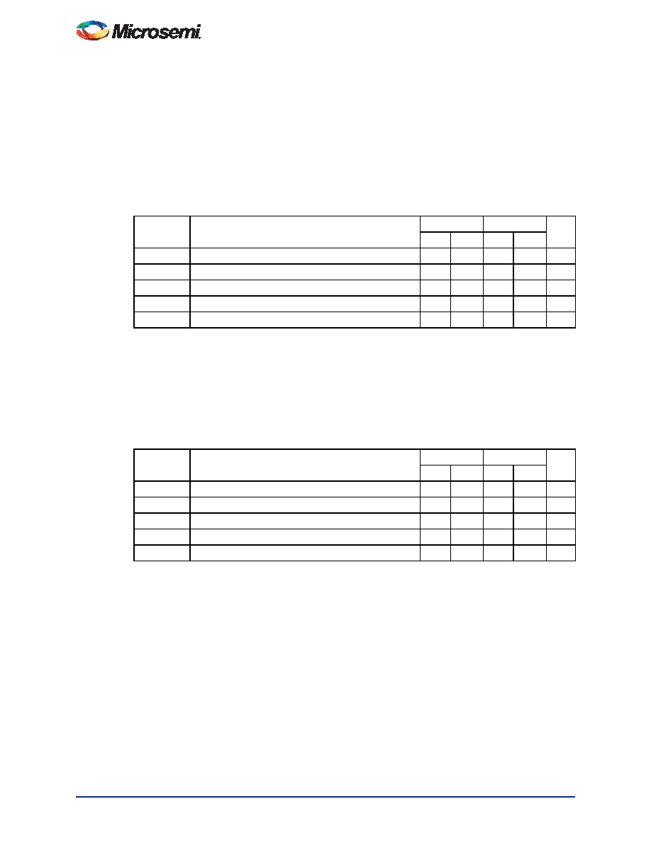
Table 2-204 A3P250L Global Resource – Applies to 1.5 V DC Core Voltage
Commercial-Case Conditions: TJ = 70°C, VCC = 1.425 V
Parameter
Description
–1
Std.
Units
Min.1 Max.2 Min.1 Max.2
tRCKL
Input Low Delay for Global Clock
0.82
1.06
0.96
1.25
ns
tRCKH
Input High Delay for Global Clock
0.80
1.09
0.94
1.28
ns
tRCKMPWH
Minimum Pulse Width High for Global Clock
0.75
0.88
ns
tRCKMPWL
Minimum Pulse Width Low for Global Clock
0.85
1.00
ns
tRCKSW
Maximum Skew for Global Clock
0.29
0.34
ns
Notes:
1. Value reflects minimum load. The delay is measured from the CCC output to the clock pin of a sequential
element, located in a lightly loaded row (single element is connected to the global net).
2. Value reflects maximum load. The delay is measured on the clock pin of the farthest sequential element,
located in a fully loaded row (all available flip-flops are connected to the global net in the row).
3. For specific junction temperature and voltage supply levels, refer to Table 2-6 on page 2-7 for derating
values.
Table 2-205 A3P250L Global Resource – Applies to 1.2 V DC Core Voltage
Commercial-Case Conditions: TJ = 70°C, VCC = 1.14 V
Parameter
Description
–1
Std.
Units
Min.1 Max.2 Min.1 Max.2
tRCKL
Input Low Delay for Global Clock
1.40
1.68
1.64
1.97
ns
tRCKH
Input High Delay for Global Clock
1.38
1.71
1.62
2.01
ns
tRCKMPWH
Minimum Pulse Width High for Global Clock
1.05
1.24
ns
tRCKMPWL
Minimum Pulse Width Low for Global Clock
1.23
1.44
ns
tRCKSW
Maximum Skew for Global Clock
0.33
0.39
ns
Notes:
1. Value reflects minimum load. The delay is measured from the CCC output to the clock pin of a sequential
element, located in a lightly loaded row (single element is connected to the global net).
2. Value reflects maximum load. The delay is measured on the clock pin of the farthest sequential element,
located in a fully loaded row (all available flip-flops are connected to the global net in the row).
3. For specific junction temperature and voltage supply levels, refer to Table 2-6 on page 2-7 for derating
values.
相关PDF资料 |
PDF描述 |
|---|---|
| A3P600L-PQ208I | IC FPGA 1KB FLASH 600K 208-PQFP |
| M1A3P600-2PQG208I | IC FPGA 1KB FLASH 600K 208-PQFP |
| M1A3P600L-PQG208I | IC FPGA 1KB FLASH 600K 208-PQFP |
| M1A3P600-2PQ208I | IC FPGA 1KB FLASH 600K 208-PQFP |
| EP20K100EQC208-3 | IC APEX 20KE FPGA 100K 208-PQFP |
相关代理商/技术参数 |
参数描述 |
|---|---|
| A3P600-PQ144 | 制造商:ACTEL 制造商全称:Actel Corporation 功能描述:ProASIC3 Flash Family FPGAs |
| A3P600-PQ144ES | 制造商:ACTEL 制造商全称:Actel Corporation 功能描述:ProASIC3 Flash Family FPGAs |
| A3P600-PQ144I | 制造商:ACTEL 制造商全称:Actel Corporation 功能描述:ProASIC3 Flash Family FPGAs |
| A3P600-PQ144PP | 制造商:ACTEL 制造商全称:Actel Corporation 功能描述:ProASIC3 Flash Family FPGAs |
| A3P600-PQ208 | 功能描述:IC FPGA 1KB FLASH 600K 208-PQFP RoHS:否 类别:集成电路 (IC) >> 嵌入式 - FPGA(现场可编程门阵列) 系列:ProASIC3 标准包装:90 系列:ProASIC3 LAB/CLB数:- 逻辑元件/单元数:- RAM 位总计:36864 输入/输出数:157 门数:250000 电源电压:1.425 V ~ 1.575 V 安装类型:表面贴装 工作温度:-40°C ~ 125°C 封装/外壳:256-LBGA 供应商设备封装:256-FPBGA(17x17) |
发布紧急采购,3分钟左右您将得到回复。