- 您现在的位置:买卖IC网 > PDF目录164971 > A3PN125-VQ100I FPGA, 3072 CLBS, 125000 GATES, PQFP100 PDF资料下载
参数资料
| 型号: | A3PN125-VQ100I |
| 元件分类: | FPGA |
| 英文描述: | FPGA, 3072 CLBS, 125000 GATES, PQFP100 |
| 封装: | 14 X 14 MM, 1.20 MM HEIGHT, 0.50 MM PITCH, VQFP-100 |
| 文件页数: | 10/106页 |
| 文件大小: | 3324K |
| 代理商: | A3PN125-VQ100I |
第1页第2页第3页第4页第5页第6页第7页第8页第9页当前第10页第11页第12页第13页第14页第15页第16页第17页第18页第19页第20页第21页第22页第23页第24页第25页第26页第27页第28页第29页第30页第31页第32页第33页第34页第35页第36页第37页第38页第39页第40页第41页第42页第43页第44页第45页第46页第47页第48页第49页第50页第51页第52页第53页第54页第55页第56页第57页第58页第59页第60页第61页第62页第63页第64页第65页第66页第67页第68页第69页第70页第71页第72页第73页第74页第75页第76页第77页第78页第79页第80页第81页第82页第83页第84页第85页第86页第87页第88页第89页第90页第91页第92页第93页第94页第95页第96页第97页第98页第99页第100页第101页第102页第103页第104页第105页第106页
ProASIC3 nano Flash FPGAs
R e visio n 8
1 -5
capability is unique to the Actel ProASIC3 family of third-generation architecture flash FPGAs. VersaTiles
are connected with any of the four levels of routing hierarchy. Flash switches are distributed throughout
the device to provide nonvolatile, reconfigurable interconnect programming. Maximum core utilization is
possible for virtually any design.
In addition, extensive on-chip programming circuitry allows for rapid, single-voltage (3.3 V) programming
of ProASIC3 nano devices via an IEEE 1532 JTAG interface.
VersaTiles
The ProASIC3 nano core consists of VersaTiles, which have been enhanced beyond the ProASICPLUS
core tiles. The ProASIC3 nano VersaTile supports the following:
All 3-input logic functions—LUT-3 equivalent
Latch with clear or set
D-flip-flop with clear or set
Enable D-flip-flop with clear or set
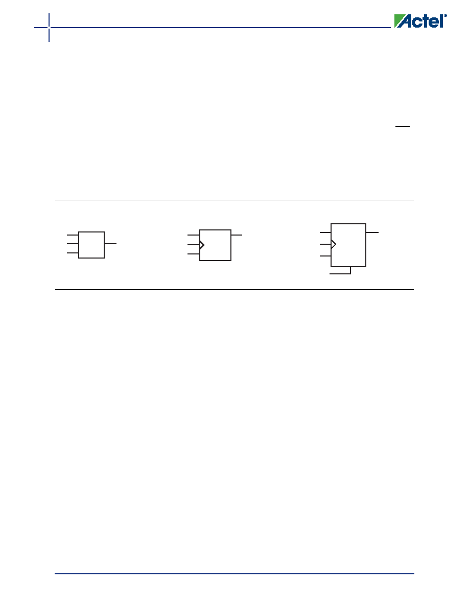
Refer to Figure 1-5 for VersaTile configurations.
User Nonvolatile FlashROM
Actel ProASIC3 nano devices have 1 kbit of on-chip, user-accessible, nonvolatile FlashROM. The
FlashROM can be used in diverse system applications:
Internet protocol addressing (wireless or fixed)
System calibration settings
Device serialization and/or inventory control
Subscription-based business models (for example, set-top boxes)
Secure key storage for secure communications algorithms
Asset management/tracking
Date stamping
Version management
The FlashROM is written using the standard ProASIC3 nano IEEE 1532 JTAG programming interface.
The core can be individually programmed (erased and written), and on-chip AES decryption can be used
selectively to securely load data over public networks (except in the A3PN030 and smaller devices), as in
security keys stored in the FlashROM for a user design.
The FlashROM can be programmed via the JTAG programming interface, and its contents can be read
back either through the JTAG programming interface or via direct FPGA core addressing. Note that the
FlashROM can only be programmed from the JTAG interface and cannot be programmed from the
internal logic array.
The FlashROM is programmed as 8 banks of 128 bits; however, reading is performed on a byte-by-byte
basis using a synchronous interface. A 7-bit address from the FPGA core defines which of the 8 banks
and which of the 16 bytes within that bank are being read. The three most significant bits (MSBs) of the
FlashROM address determine the bank, and the four least significant bits (LSBs) of the FlashROM
address define the byte.
Figure 1-5
VersaTile Configurations
X1
Y
X2
X3
LUT-3
Data
Y
CLK
Enable
CLR
D-FF
Data
Y
CLK
CLR
D-FF
LUT-3 Equivalent
D-Flip-Flop with Clear or Set
Enable D-Flip-Flop with Clear or Set
相关PDF资料 |
PDF描述 |
|---|---|
| A3PN125-VQ100 | FPGA, 3072 CLBS, 125000 GATES, PQFP100 |
| A3PN125-VQG100I | FPGA, 3072 CLBS, 125000 GATES, PQFP100 |
| A3PN125-VQG100 | FPGA, 3072 CLBS, 125000 GATES, PQFP100 |
| A3PN125-Z1VQ100I | FPGA, 3072 CLBS, 125000 GATES, PQFP100 |
| A3PN125-Z1VQ100 | FPGA, 3072 CLBS, 125000 GATES, PQFP100 |
相关代理商/技术参数 |
参数描述 |
|---|---|
| A3PN125-VQG100 | 功能描述:IC FPGA NANO 1024MAC 100VQFP RoHS:是 类别:集成电路 (IC) >> 嵌入式 - FPGA(现场可编程门阵列) 系列:ProASIC3 nano 标准包装:60 系列:XP LAB/CLB数:- 逻辑元件/单元数:10000 RAM 位总计:221184 输入/输出数:244 门数:- 电源电压:1.71 V ~ 3.465 V 安装类型:表面贴装 工作温度:0°C ~ 85°C 封装/外壳:388-BBGA 供应商设备封装:388-FPBGA(23x23) 其它名称:220-1241 |
| A3PN125-VQG100I | 功能描述:IC FPGA NANO 125K GATES 100-VQFP RoHS:是 类别:集成电路 (IC) >> 嵌入式 - FPGA(现场可编程门阵列) 系列:ProASIC3 nano 标准包装:152 系列:IGLOO PLUS LAB/CLB数:- 逻辑元件/单元数:792 RAM 位总计:- 输入/输出数:120 门数:30000 电源电压:1.14 V ~ 1.575 V 安装类型:表面贴装 工作温度:-40°C ~ 85°C 封装/外壳:289-TFBGA,CSBGA 供应商设备封装:289-CSP(14x14) |
| A3PN125-Z1VQ100 | 功能描述:IC FPGA NANO 125K GATES 100-VQFP RoHS:否 类别:集成电路 (IC) >> 嵌入式 - FPGA(现场可编程门阵列) 系列:ProASIC3 nano 标准包装:152 系列:IGLOO PLUS LAB/CLB数:- 逻辑元件/单元数:792 RAM 位总计:- 输入/输出数:120 门数:30000 电源电压:1.14 V ~ 1.575 V 安装类型:表面贴装 工作温度:-40°C ~ 85°C 封装/外壳:289-TFBGA,CSBGA 供应商设备封装:289-CSP(14x14) |
| A3PN125-Z1VQ100I | 功能描述:IC FPGA NANO 125K GATES 100-VQFP RoHS:否 类别:集成电路 (IC) >> 嵌入式 - FPGA(现场可编程门阵列) 系列:ProASIC3 nano 标准包装:152 系列:IGLOO PLUS LAB/CLB数:- 逻辑元件/单元数:792 RAM 位总计:- 输入/输出数:120 门数:30000 电源电压:1.14 V ~ 1.575 V 安装类型:表面贴装 工作温度:-40°C ~ 85°C 封装/外壳:289-TFBGA,CSBGA 供应商设备封装:289-CSP(14x14) |
| A3PN125-Z1VQG100 | 功能描述:IC FPGA NANO 125K GATES 100-VQFP RoHS:是 类别:集成电路 (IC) >> 嵌入式 - FPGA(现场可编程门阵列) 系列:ProASIC3 nano 标准包装:152 系列:IGLOO PLUS LAB/CLB数:- 逻辑元件/单元数:792 RAM 位总计:- 输入/输出数:120 门数:30000 电源电压:1.14 V ~ 1.575 V 安装类型:表面贴装 工作温度:-40°C ~ 85°C 封装/外壳:289-TFBGA,CSBGA 供应商设备封装:289-CSP(14x14) |
发布紧急采购,3分钟左右您将得到回复。