- 您现在的位置:买卖IC网 > PDF目录22010 > A42MX16-PLG84 (Microsemi SoC)IC FPGA 140I/O 84PLCC PDF资料下载
参数资料
| 型号: | A42MX16-PLG84 |
| 厂商: | Microsemi SoC |
| 文件页数: | 13/142页 |
| 文件大小: | 0K |
| 描述: | IC FPGA 140I/O 84PLCC |
| 标准包装: | 16 |
| 系列: | MX |
| 输入/输出数: | 72 |
| 门数: | 24000 |
| 电源电压: | 3 V ~ 3.6 V,4.75 V ~ 5.25 V |
| 安装类型: | 表面贴装 |
| 工作温度: | 0°C ~ 70°C |
| 封装/外壳: | 84-LCC(J 形引线) |
| 供应商设备封装: | 84-PLCC(29.31x29.31) |
| 其它名称: | 1100-1053 |
第1页第2页第3页第4页第5页第6页第7页第8页第9页第10页第11页第12页当前第13页第14页第15页第16页第17页第18页第19页第20页第21页第22页第23页第24页第25页第26页第27页第28页第29页第30页第31页第32页第33页第34页第35页第36页第37页第38页第39页第40页第41页第42页第43页第44页第45页第46页第47页第48页第49页第50页第51页第52页第53页第54页第55页第56页第57页第58页第59页第60页第61页第62页第63页第64页第65页第66页第67页第68页第69页第70页第71页第72页第73页第74页第75页第76页第77页第78页第79页第80页第81页第82页第83页第84页第85页第86页第87页第88页第89页第90页第91页第92页第93页第94页第95页第96页第97页第98页第99页第100页第101页第102页第103页第104页第105页第106页第107页第108页第109页第110页第111页第112页第113页第114页第115页第116页第117页第118页第119页第120页第121页第122页第123页第124页第125页第126页第127页第128页第129页第130页第131页第132页第133页第134页第135页第136页第137页第138页第139页第140页第141页第142页
40MX and 42MX FPGA Families
Re vi s i on 11
1-7
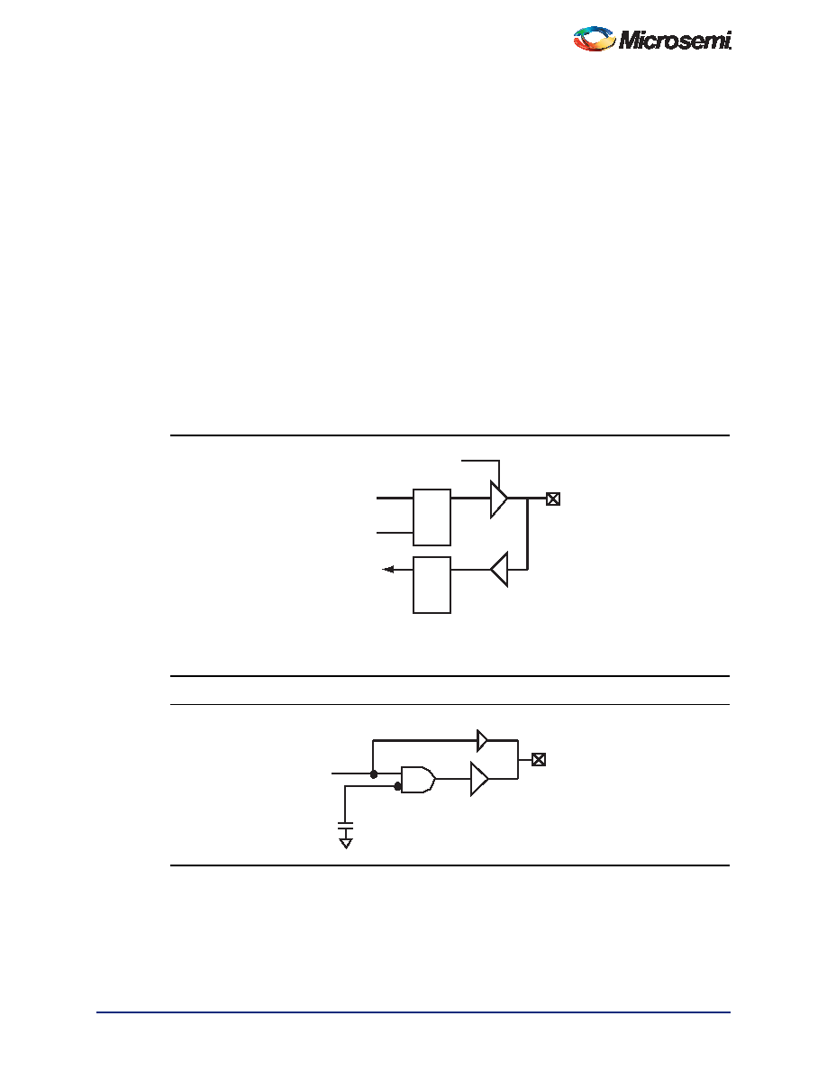
MultiPlex I/O Modules
42MX devices feature Multiplex I/Os and support 5.0V, 3.3V, and mixed 3.3V/5.0V operations.
The MultiPlex I/O modules provide the interface between the device pins and the logic array. Figure 1-9
is a block diagram of the 42MX I/O module. A variety of user functions, determined by a library macro
selection, can be implemented in the module. (Refer to the Antifuse Macro Library Guide for more
information.) All 42MX I/O modules contain tristate buffers, with input and output latches that can be
configured for input, output, or bidirectional operation.
All 42MX devices contain flexible I/O structures, where each output pin has a dedicated output-enable
control (Figure 1-9). The I/O module can be used to latch input or output data, or both, providing fast set-
up time. In addition, the Designer software tools can build a D-type flip-flop using a C-module combined
with an I/O module to register input and output signals. Refer to the Antifuse Macro Library Guide for
more details.
A42MX24 and A42MX36 devices also offer selectable PCI output drives, enabling 100% compliance with
version 2.1 of the PCI specification. For low-power systems, all inputs and outputs are turned off to
reduce current consumption to below 500
μA.
To achieve 5.0V or 3.3V PCI-compliant output drives on A42MX24 and A42MX36 devices, a chip-wide
PCI fuse is programmed via the Device Selection Wizard in the Designer software (Figure 1-10). When
the PCI fuse is not programmed, the output drive is standard.
Designer software development tools provide a design library of I/O macro functions that can implement
all I/O configurations supported by the MX FPGAs.
Note:
*Can be configured as a Latch or D Flip-Flop (Using
C-Module)
Figure 1-9
42MX I/O Module
Figure 1-10 PCI Output Structure of A42MX24 and A42MX36 Devices
Q
D
From Array
To Array
G/CLK*
Q
D
PAD
EN
Signal
PCI Enable
PCI
Fuse
Drive
STD
Output
相关PDF资料 |
PDF描述 |
|---|---|
| ESC26DTEN | CONN EDGECARD 52POS .100 EYELET |
| RSO-2412D/H3 | CONV DC/DC 1W 18-36VIN +/-12VOUT |
| ESC26DTEH | CONN EDGECARD 52POS .100 EYELET |
| DB25P065HTXLF | CONN DSUB PLUG 25POS SLD CUP |
| ACC30DRAS | CONN EDGECARD 60POS .100 R/A DIP |
相关代理商/技术参数 |
参数描述 |
|---|---|
| A42MX16-PLG84A | 功能描述:IC FPGA MX SGL CHIP 24K 84-PLCC RoHS:是 类别:集成电路 (IC) >> 嵌入式 - FPGA(现场可编程门阵列) 系列:MX 标准包装:40 系列:SX-A LAB/CLB数:6036 逻辑元件/单元数:- RAM 位总计:- 输入/输出数:360 门数:108000 电源电压:2.25 V ~ 5.25 V 安装类型:表面贴装 工作温度:0°C ~ 70°C 封装/外壳:484-BGA 供应商设备封装:484-FPBGA(27X27) |
| A42MX16-PLG84I | 功能描述:IC FPGA MX SGL CHIP 24K 84-PLCC RoHS:是 类别:集成电路 (IC) >> 嵌入式 - FPGA(现场可编程门阵列) 系列:MX 标准包装:40 系列:SX-A LAB/CLB数:6036 逻辑元件/单元数:- RAM 位总计:- 输入/输出数:360 门数:108000 电源电压:2.25 V ~ 5.25 V 安装类型:表面贴装 工作温度:0°C ~ 70°C 封装/外壳:484-BGA 供应商设备封装:484-FPBGA(27X27) |
| A42MX16-PLG84M | 制造商:Microsemi Corporation 功能描述:FPGA 42MX Family 24K Gates 608 Cells 103MHz/172MHz 0.45um (CMOS) Technology 3.3V/5V 84-Pin PLCC 制造商:Microsemi SOC Products Group 功能描述:FPGA 24K GATES 608 CELLS 103MHZ/172MHZ 0.45UM 3.3V/5V 84PLCC - Rail/Tube 制造商:Microsemi Corporation 功能描述:IC FPGA MX SGL CHIP 24K 84-PLCC |
| A42MX16-PQ100 | 功能描述:IC FPGA MX SGL CHIP 24K 100-PQFP RoHS:否 类别:集成电路 (IC) >> 嵌入式 - FPGA(现场可编程门阵列) 系列:MX 标准包装:40 系列:SX-A LAB/CLB数:6036 逻辑元件/单元数:- RAM 位总计:- 输入/输出数:360 门数:108000 电源电压:2.25 V ~ 5.25 V 安装类型:表面贴装 工作温度:0°C ~ 70°C 封装/外壳:484-BGA 供应商设备封装:484-FPBGA(27X27) |
| A42MX16-PQ100A | 功能描述:IC FPGA MX SGL CHIP 24K 100-PQFP RoHS:否 类别:集成电路 (IC) >> 嵌入式 - FPGA(现场可编程门阵列) 系列:MX 标准包装:40 系列:SX-A LAB/CLB数:6036 逻辑元件/单元数:- RAM 位总计:- 输入/输出数:360 门数:108000 电源电压:2.25 V ~ 5.25 V 安装类型:表面贴装 工作温度:0°C ~ 70°C 封装/外壳:484-BGA 供应商设备封装:484-FPBGA(27X27) |
发布紧急采购,3分钟左右您将得到回复。