参数资料
| 型号: | A42MX16-PQG208I |
| 厂商: | Microsemi SoC |
| 文件页数: | 132/142页 |
| 文件大小: | 0K |
| 描述: | IC FPGA MX SGL CHIP 24K 208-PQFP |
| 标准包装: | 24 |
| 系列: | MX |
| 输入/输出数: | 140 |
| 门数: | 24000 |
| 电源电压: | 3 V ~ 3.6 V,4.5 V ~ 5.5 V |
| 安装类型: | 表面贴装 |
| 工作温度: | -40°C ~ 85°C |
| 封装/外壳: | 208-BFQFP |
| 供应商设备封装: | 208-PQFP(28x28) |
第1页第2页第3页第4页第5页第6页第7页第8页第9页第10页第11页第12页第13页第14页第15页第16页第17页第18页第19页第20页第21页第22页第23页第24页第25页第26页第27页第28页第29页第30页第31页第32页第33页第34页第35页第36页第37页第38页第39页第40页第41页第42页第43页第44页第45页第46页第47页第48页第49页第50页第51页第52页第53页第54页第55页第56页第57页第58页第59页第60页第61页第62页第63页第64页第65页第66页第67页第68页第69页第70页第71页第72页第73页第74页第75页第76页第77页第78页第79页第80页第81页第82页第83页第84页第85页第86页第87页第88页第89页第90页第91页第92页第93页第94页第95页第96页第97页第98页第99页第100页第101页第102页第103页第104页第105页第106页第107页第108页第109页第110页第111页第112页第113页第114页第115页第116页第117页第118页第119页第120页第121页第122页第123页第124页第125页第126页第127页第128页第129页第130页第131页当前第132页第133页第134页第135页第136页第137页第138页第139页第140页第141页第142页
40MX and 42MX FPGA Families
Re vi s i on 11
1-5
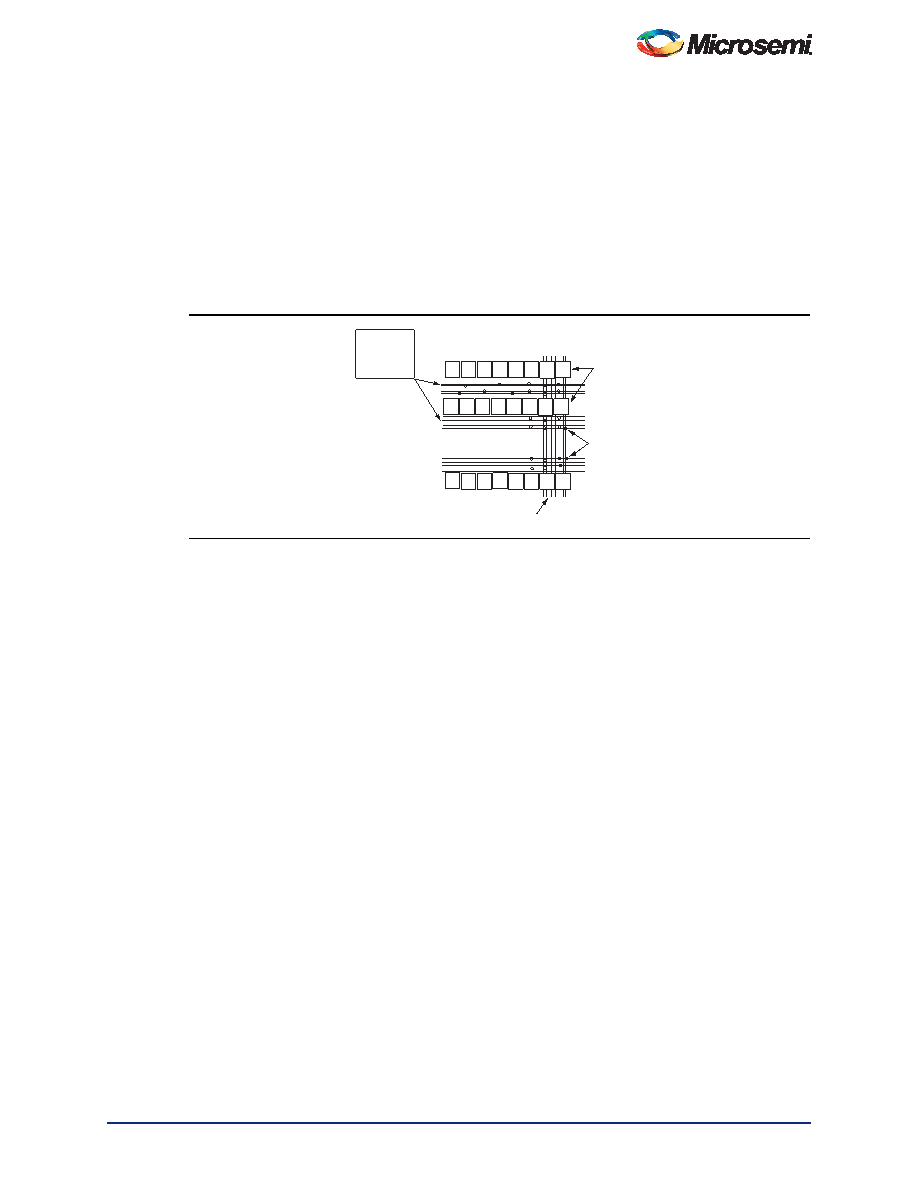
uncommitted and can be assigned during routing. Each output segment spans four channels (two above
and two below), except near the top and bottom of the array, where edge effects occur. Long vertical
tracks contain either one or two segments. An example of vertical routing tracks and segments is shown
in Figure 1-6.
Antifuse Structures
An antifuse is a "normally open" structure. The use of antifuses to implement a programmable logic
device results in highly testable structures as well as efficient programming algorithms. There are no pre-
existing connections; temporary connections can be made using pass transistors. These temporary
connections can isolate individual antifuses to be programmed and individual circuit structures to be
tested, which can be done before and after programming. For instance, all metal tracks can be tested for
continuity and shorts between adjacent tracks, and the functionality of all logic modules can be verified.
Clock Networks
The 40MX devices have one global clock distribution network (CLK). A signal can be put on the CLK
network by being routed through the CLKBUF buffer.
In 42MX devices, there are two low-skew, high-fanout clock distribution networks, referred to as CLKA
and CLKB. Each network has a clock module (CLKMOD) that can select the source of the clock signal
from any of the following (Figure 1-7 on page 1-6):
Externally from the CLKA pad, using CLKBUF buffer
Externally from the CLKB pad, using CLKBUF buffer
Internally from the CLKINTA input, using CLKINT buffer
Internally from the CLKINTB input, using CLKINT buffer
The clock modules are located in the top row of I/O modules. Clock drivers and a dedicated horizontal
clock track are located in each horizontal routing channel.
Clock input pads in both 40MX and 42MX devices can also be used as normal I/Os, bypassing the clock
networks.
The A42MX36 device has four additional register control resources, called quadrant clock networks
(Figure 1-8 on page 1-6). Each quadrant clock provides a local, high-fanout resource to the contiguous
logic modules within its quadrant of the device. Quadrant clock signals can originate from specific I/O
Figure 1-6
MX Routing Structure
Segmented
Horizontal
Routing
Logic
Modules
Antifuses
Vertical Routing Tracks
相关PDF资料 |
PDF描述 |
|---|---|
| A42MX16-2PQ100 | IC FPGA MX SGL CHIP 24K 100-PQFP |
| A1020B-PQ100C | IC FPGA 2K GATES 100-PQFP COM |
| 5745653-5 | CONN BACKSHELL DB25 90DEG METAL |
| A1020B-PQG100C | IC FPGA 2K GATES 100-PQFP COM |
| 5745653-4 | CONN BACKSHELL DB25 90DEG METAL |
相关代理商/技术参数 |
参数描述 |
|---|---|
| A42MX16-PQG208M | 制造商:Microsemi Corporation 功能描述:FPGA 24K GATES 608 CELLS 103MHZ/172MHZ 0.45UM 3.3V/5V 208PQF - Trays 制造商:Microsemi Corporation 功能描述:IC FPGA 140 I/O 208PQFP |
| A42MX16-TQ176 | 功能描述:IC FPGA MX SGL CHIP 24K 176-TQFP RoHS:否 类别:集成电路 (IC) >> 嵌入式 - FPGA(现场可编程门阵列) 系列:MX 标准包装:40 系列:SX-A LAB/CLB数:6036 逻辑元件/单元数:- RAM 位总计:- 输入/输出数:360 门数:108000 电源电压:2.25 V ~ 5.25 V 安装类型:表面贴装 工作温度:0°C ~ 70°C 封装/外壳:484-BGA 供应商设备封装:484-FPBGA(27X27) |
| A42MX16-TQ176A | 功能描述:IC FPGA MX SGL CHIP 24K 176-TQFP RoHS:否 类别:集成电路 (IC) >> 嵌入式 - FPGA(现场可编程门阵列) 系列:MX 标准包装:40 系列:SX-A LAB/CLB数:6036 逻辑元件/单元数:- RAM 位总计:- 输入/输出数:360 门数:108000 电源电压:2.25 V ~ 5.25 V 安装类型:表面贴装 工作温度:0°C ~ 70°C 封装/外壳:484-BGA 供应商设备封装:484-FPBGA(27X27) |
| A42MX16-TQ176I | 功能描述:IC FPGA MX SGL CHIP 24K 176-TQFP RoHS:否 类别:集成电路 (IC) >> 嵌入式 - FPGA(现场可编程门阵列) 系列:MX 标准包装:40 系列:SX-A LAB/CLB数:6036 逻辑元件/单元数:- RAM 位总计:- 输入/输出数:360 门数:108000 电源电压:2.25 V ~ 5.25 V 安装类型:表面贴装 工作温度:0°C ~ 70°C 封装/外壳:484-BGA 供应商设备封装:484-FPBGA(27X27) |
| A42MX16-TQ176M | 制造商:Microsemi Corporation 功能描述:FPGA 24K GATES 608 CELLS 103MHZ/172MHZ 0.45UM 3.3V/5V 176TQF - Trays 制造商:Microsemi Corporation 功能描述:IC FPGA MX SGL CHIP 24K 176-TQFP 制造商:Microsemi Corporation 功能描述:IC FPGA 140 I/O 176TQFP |
发布紧急采购,3分钟左右您将得到回复。